

Hold-time optimization circuit and receiver with the same
a technology of hold time optimization and receiver, which is applied in the direction of pulse generator, pulse manipulation, pulse technique, etc., can solve the problems of erroneous data cycle capture of digital circuits and difficulty for designers to set hold time appropriately, and achieve the effect of reducing delay time and reducing delay tim
- Summary
- Abstract
- Description
- Claims
- Application Information
AI Technical Summary
Benefits of technology
Problems solved by technology
Method used
Image

Examples
Embodiment Construction
[0020]In order to illustrate the purposes, features and advantages of the invention, the embodiments and figures of the invention will be described in detail as follows.
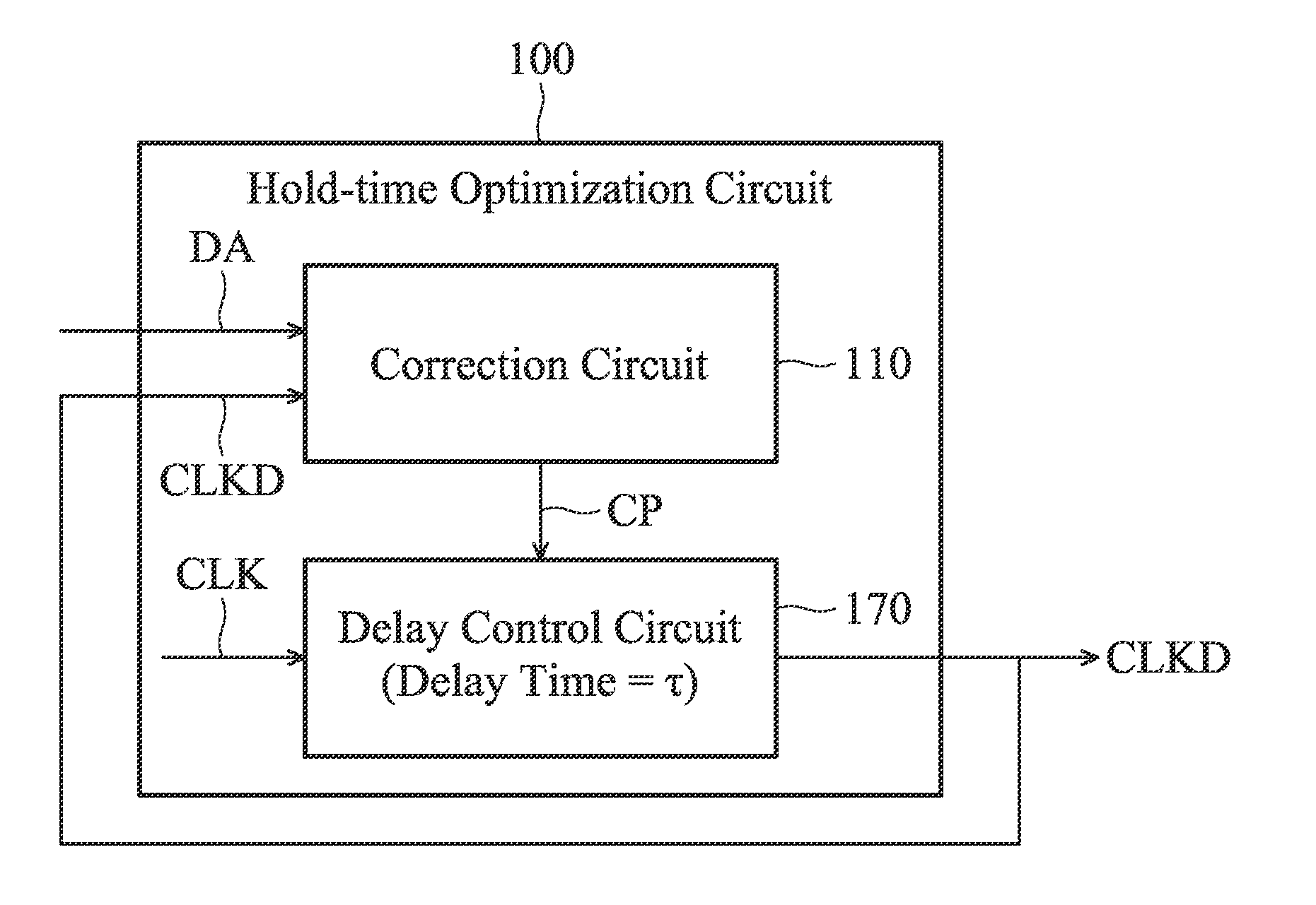
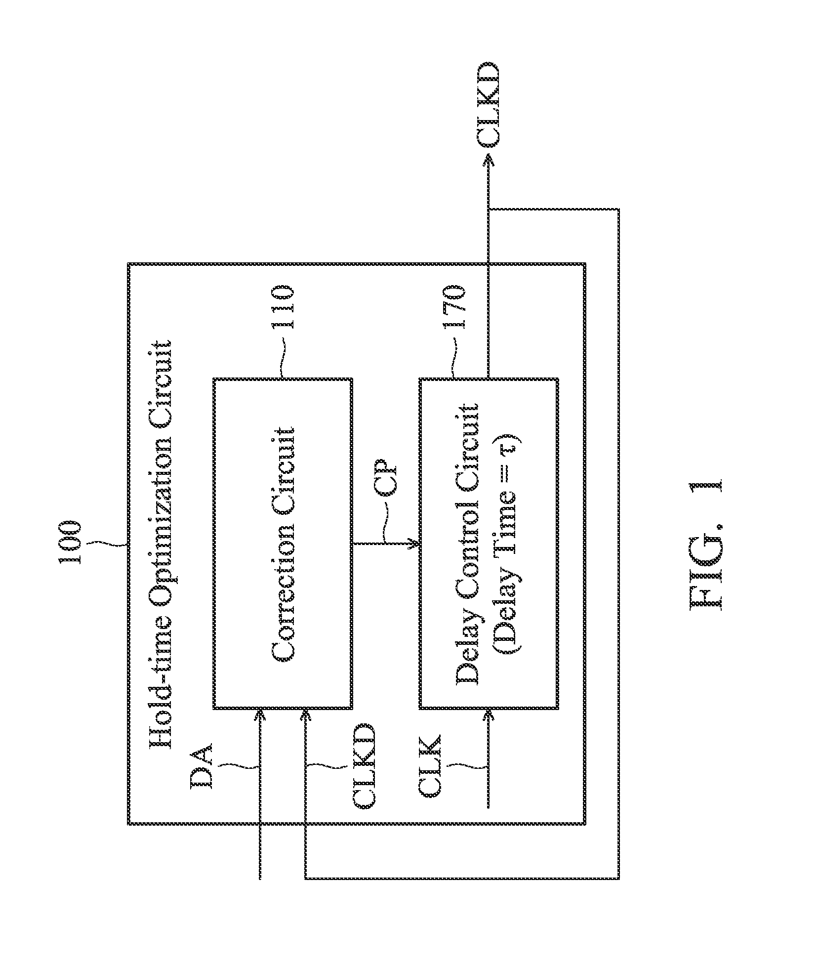
[0021]FIG. 1 is a diagram of a hold-time optimization circuit 100 according to an embodiment of the invention. As shown in FIG. 1, the hold-time optimization circuit 100 at least includes a correction circuit 110 and a delay control circuit 170. The hold-time optimization circuit 100 may be used in a digital circuit, such as a low-power digital integrated circuit for sampling data. A data signal DA and a clock signal CLK of the digital circuit may be applied to the hold-time optimization circuit 100. The delay control circuit 170 delays the clock signal CLK for delay time τ so as to generate a delay clock signal CLKD. That is, the clock signal CLK and the delay clock signal CLKD may have identical waveforms but different phases. The correction circuit 110 generates a correction pulse signal CP according to the data s...
PUM
 Abstract
Description
Claims
Application Information