

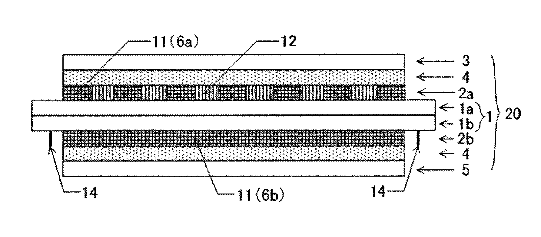
Optically transparent electrode
a transparent electrode and transparent technology, applied in the field of optically transparent electrodes, can solve the problems of increased electrical resistance, low total light transmittance, low flexibility of conductive layers, etc., and achieve the effects of high total light transmittance, low cost, and low cos
- Summary
- Abstract
- Description
- Claims
- Application Information
AI Technical Summary
Benefits of technology
Problems solved by technology
Method used
Image

Examples
example 1
[0071]As an optically transparent base material, a 100-μm-thick polyethylene terephthalate film was used. The total light transmittance of this optically transparent base material was 91%.
[0072]Next, in accordance with the following formulation, a physical development nuclei coating liquid was prepared, applied onto one side of the optically transparent base material, and dried to provide a physical development nuclei layer.
[0073]
Liquid APalladium chloride5gHydrochloric acid40mLDistilled water1000mLLiquid BSodium sulfide8.6gDistilled water1000mL
[0074]Liquid A and Liquid B were mixed with stirring for 30 minutes, and then passed through a column filled up with an ion exchange resin to give a palladium sulfide sol.
[0075]
per m2 of silver halide photosensitive materialThe above-prepared palladium sulfide sol0.4mg2 mass % glyoxal aqueous solution0.2mLSurfactant (S-1)4mgDenacol EX-83050mg(Polyethylene glycol diglycidyl ether madeby Nagase Chemtex Corp.)10 mass % SP-200 aqueous solution0.5...
example 2 , example 3
Example 2, Example 3, Comparative Examples 1 to 5>
[0082]The same procedure was performed as in Example 1 except that transparent manuscripts in which the values of k1, j1, and angle 1 in FIGS. 7, and k2, j2, and angle 2 in FIG. 8 are those shown in Table 1 were used, and optically transparent electrodes of Example 2, Example 3, and Comparative Examples 1 to 5 were obtained. In all of the optically transparent electrodes, M was 15 mm and L was 20 mm.
[0083]The obtained optically transparent electrodes of Examples 1 to 3, and Comparative Examples 1 to 5 were evaluated for the occurrence of moire, the total light transmittance, and the stability of electrical resistance values by the method shown below. The results are shown in Table 1.
[0084]The obtained optically transparent electrode was placed on the screen of a 23″ wide LCD monitor (RDT234WK (BK) made by Mitsubishi Electric) displaying solid white, and was evaluated based on the following criteria. Poor and Very Poor are not practic...
PUM
 Abstract
Description
Claims
Application Information