Semiconductor device and method of manufacturing the same

a semiconductor and semiconductor technology, applied in semiconductor devices, diodes, electrical devices, etc., can solve the problems of inability to easily convert nitride semiconductors into p-type semiconductors, and inability to obtain sbd which exhibits preferable rectification characteristics

Active Publication Date: 2016-02-04
TOYOTA CENT RES & DEV LAB INC +1
View PDF2 Cites 8 Cited by
  • Summary
  • Abstract
  • Description
  • Claims
  • Application Information

AI Technical Summary

Benefits of technology

[0029]Alternatively, in at least a part of the region where the anode electrode of the SBD is to be formed, the third nitride semiconductor layer may be wet-etched in the removing of the third nitride semiconductor layer to expose the second nitride semiconductor layer. When the third nitride semiconductor layer is wet-etched, the exposed surface of t

Problems solved by technology

A nitride semiconductor cannot be easily converted into a p-type semiconductor by injecting acceptor impurities therein.
However, even though the above operations are actually performed, the SBD which exhibits preferable rect

Method used


Image

  • Semiconductor device and method of manufacturing the same
  • Semiconductor device and method of manufacturing the same
  • Semiconductor device and method of manufacturing the same

Examples


first embodiment

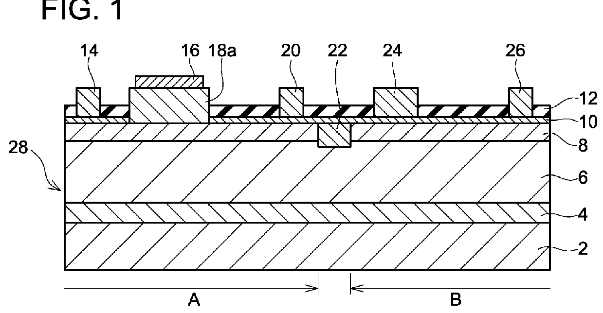
[0049]As shown in FIG. 1, in a semiconductor device according to a first embodiment, a HEMT and an SBD are formed on one same nitride semiconductor substrate 28. The HEMT is formed in a region A, and the SBD is formed in a region B.

[0050]The nitride semiconductor substrate 28 according to the embodiment includes a laminated structure configured by a substrate 2, a buffer layer 4 crystal-grown on a front surface of the substrate 2, a first nitride semiconductor layer 6 crystal-grown on a front surface of the buffer layer 4, a second nitride semiconductor layer 8 crystal-grown on a front surface of the first nitride semiconductor layer 6, and a third nitride semiconductor layer 18 crystal-grown on a front surface of the second nitride semiconductor layer 8.

[0051]FIG. 1 shows a state after the third nitride semiconductor layer 18 is etched and removed in a region except for a region in which a gate electrode 16 (which will be described later) is formed, and shows only a remaining regio...

second embodiment

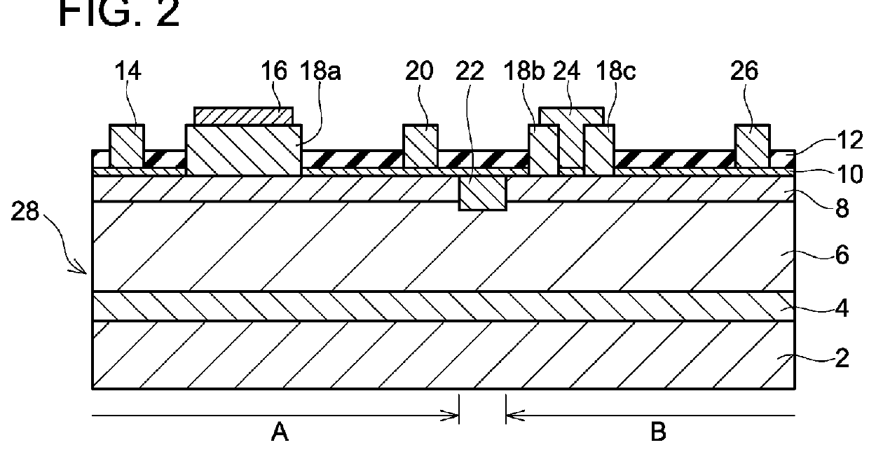
[0065]The same reference numerals as in the first embodiment denote the same members in the second embodiment to omit the same explanations. Only different aspects between the first embodiment and the second embodiment will be described below.

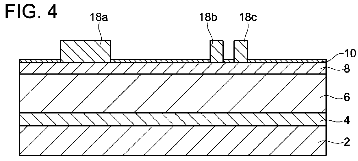
[0066]As shown in FIG. 2, in a semiconductor device according to the second embodiment, a contact portion between the anode electrode 24 and the second nitride semiconductor layer 8 is different from that in the first embodiment. In the second embodiment, even at positions being in contact with the anode electrode 24, parts 18b and 18c of the p-type third nitride semiconductor layer 18 are caused to remain. More specifically, a structure in which the p-type third nitride semiconductor layers 18b and 18c are present on left and right sides of the contact portion between the anode electrode 24 and the second nitride semiconductor layer 8, is created.

[0067]According to the structure, when a reverse voltage is applied to the diode, a depletion laye...

third embodiment

[0077]A semiconductor device according to a third embodiment will be described below with reference to FIG. 7. The semiconductor device according to the present embodiment, as shown in FIG. 8, is manufactured by using a substrate in which a surface layer 30 of a second nitride semiconductor (hereinafter referred to as ‘second nitride semiconductor surface layer 30’) is crystal-grown between a deep layer 8 of the second nitride semiconductor (hereinafter referred to as ‘second nitride semiconductor deep layer 8’) and the third nitride semiconductor layer 18. That is, a second nitride semiconductor layer 32 is configured by the second nitride semiconductor deep layer 8 and the second nitride semiconductor surface layer 30.

[0078]In this embodiment, GaN is used as the first nitride semiconductor layer 6, i-type AlxGa1-xN is used as the second nitride semiconductor deep layer 8, AlzGawIn1-z-wN is used as the second nitride semiconductor surface layer 30, and p-type AlyGa1-yN is used as t...


PUM


Abstract

Both a HEMT and a SBD are formed on a nitride semiconductor substrate. The nitride semiconductor substrate comprises a HEMT gate structure region and an anode electrode region. A first laminated structure is formed at least in the HEMT gate structure region, and includes first to third nitride semiconductor layers. A second laminated structure is formed at least in a part of the anode electrode region, and includes first and second nitride semiconductor layers. The anode electrode contacts the front surface of the second nitride semiconductor layer. At least in a contact region in which the front surface of the second nitride semiconductor layer contacts the anode electrode, the front surface of the second nitride semiconductor layer is finished to be a surface by which the second nitride semiconductor layer forms a Schottky junction with the anode electrode.

Description

CROSS-REFERENCE TO RELATED APPLICATION[0001]This application claims priority to Japanese Patent Application No. 2014-153463 filed on Jul. 29, 2014, the contents of which are hereby incorporated by reference into the present application.TECHNICAL FIELD[0002]Disclosed herein is a technique that forms a normally-off field effect transistor and a Schottky barrier diode on a common nitride semiconductor substrate.DESCRIPTION OF RELATED ART[0003]Patent Literature 1 (Japanese Patent Application Publication No. 2011-205029) discloses a technique of forming a Schottky Barrier Diode (to be referred to as an SBD (Schottky Barrier Diode) hereinafter) and a field effect transistor (to be referred to as a HEMT (High Electron Mobility Transistor) hereinafter) that uses a potential of a gate electrode for controlling a two-dimensional electron gas generated along a heterojunction interface on a common nitride semiconductor substrate.[0004]The HEMT easily exhibits normally-on characteristics due to ...

Claims


Application Information

Patent Timeline
IPC IPC(8): H01L27/06H01L21/8232H01L29/20H01L29/205
CPCH01L27/0629H01L21/8232H01L29/205H01L29/2003H01L29/0684H01L29/47H01L29/66143H01L29/66462H01L29/778H01L29/872H01L29/7786H01L29/0619H01L29/0895H01L29/1066H01L29/66212H01L21/8252H01L27/0605
Inventor KANECHIKA, MASAKAZUUEDA, HIROYUKITOMITA, HIDEMOTO
Owner TOYOTA CENT RES & DEV LAB INC
Why Eureka
Try Eureka