Display device and manufacturing method thereof

Active Publication Date: 2016-02-04
JAPAN DISPLAY INC
View PDF2 Cites 3 Cited by
  • Summary
  • Abstract
  • Description
  • Claims
  • Application Information

AI Technical Summary

Benefits of technology

The patent text describes a problem with using polyimide for forming barrier films in organic electroluminescent elements. The temperature limitation of about 550°C makes it difficult to form a stable barrier film without compromising on film thickness or adhesion. Additionally, the low heat resistance of organic materials used for barrier films makes it hard to resist the temperatures of low-temperature polysilicon processes. The invention proposes to improve the barrier film performance to prevent degradation caused by substances such as moisture.

Problems solved by technology

Polyimide can be thermally decomposed at about 500° C. or more, which restricts the upper limit temperature in forming the barrier film on the polyimide film, and thus there is a problem that the characteristics of the barrier film may be limited.
For example, when silicon oxide or silicon nitride is formed by a CVD method under this temperature limitation, a reduced film thickness tends to result in a porous film, so that the barrier performance may be insufficient.
On the other hand, an increased film thickness can improve the barrier performance, but a time required for deposition is lengthened, so that productivity is reduced.
Moreover, the heat resistance of an organic material used for the barrier film is relatively low.
Therefore, when the temperature of a low-temperature polysilicon (LTPS) process for forming TFT is higher than the heat-resistant temperature of an organic material, it is difficult to form the barrier film on the polyimide film from the organic material.
Moreover, the barrier film has poor adhesion to an organic film such as polyimide, so that detachment of the film easily occurs.

Method used


Image

  • Display device and manufacturing method thereof
  • Display device and manufacturing method thereof
  • Display device and manufacturing method thereof

Examples


first embodiment

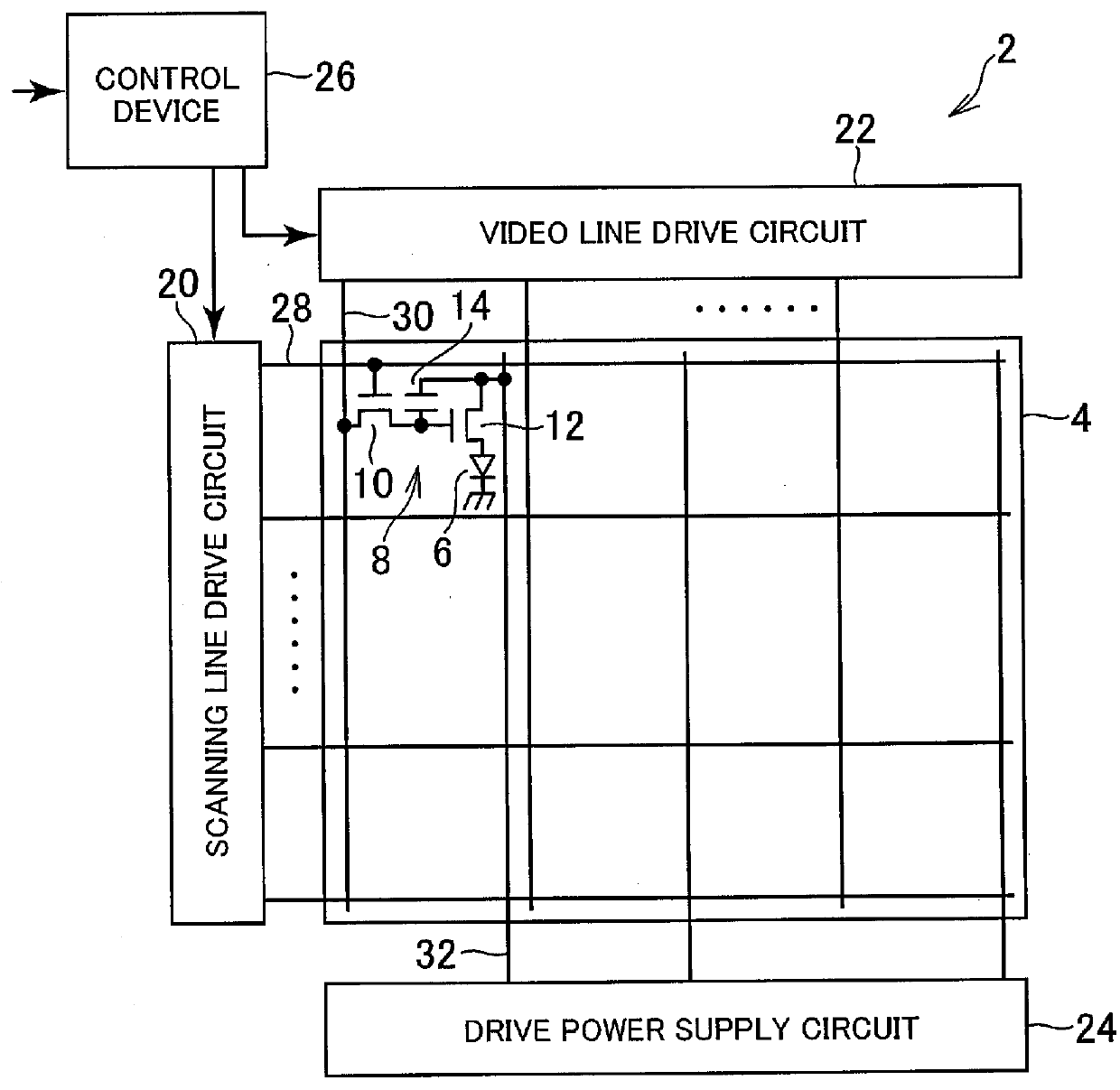
[0019]An organic EL display device is an active matrix display device, which is mounted as a display panel on a television set, a personal computer, a portable terminal, a mobile phone, or the like. FIG. 1 is a schematic view showing a schematic configuration of an organic EL display device 2 according to a first embodiment. The organic EL display device 2 includes a pixel array portion 4 that displays an image and a drive portion that drives the pixel array portion. The organic EL display device 2 is a flexible display, in which a resin film having flexibility, not a glass substrate, is used as a base material and a stacked structure of TFTs, OLEDs, and the like is formed on the base material.

[0020]In the pixel array portion 4, OLEDs 6 and pixel circuits 8 are disposed in a matrix corresponding to pixels. The pixel circuit 8 includes a plurality of TFTs 10 and 12 and a capacitor 14.

[0021]On the other hand, the drive portion includes a scanning line drive circuit 20, a video line dr...

second embodiment

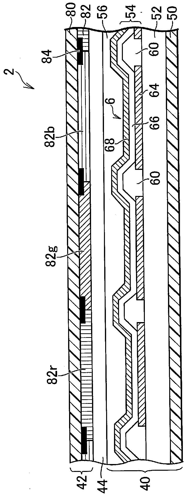
[0058]The barrier film including the impregnated barrier base material layer described in the first embodiment can be provided at a position at which the barrier film is integrated with the sealing layer 56 (sealing film) of the organic EL display device 2. Specifically, the barrier film can be provided at a position in contact with an upper or lower surface of the sealing layer 56 separately from the sealing layer 56, and in addition, the sealing layer 56 itself can be configured as the barrier film. Similarly to the sealing layer 56, the barrier film favorably blocks transmission of moisture or the like contained in the filling material 44, and protects the OLEDs.

[0059]In a second embodiment, an organic EL display device 2 in which a sealing layer 56 itself is configured as a barrier film including an impregnated barrier base material layer will be described. The organic EL display device 2 of the embodiment has a structure substantially common with that of the organic EL display ...

modified examples

[0069]The barrier film including the impregnated barrier base material layer described in the embodiments can be provided at a position other than the positions shown in the first and second embodiments.

[0070]For example, the barrier film can be provided on a filling-material-side surface of the counter substrate 42 to be bonded on the sealing layer 56 via the filling material 44.

[0071]Moreover, when, for the purpose of protecting a surface of the base material 80 for example, a film using polyethylene terephthalate (PET) as a base material and subjected to, for example, a hard coating treatment is attached to the surface, the film can be a film with the barrier film formed on a rear surface thereof.

[0072]The barrier films described in the embodiments and modified examples can be used together.

[0073]In the embodiments, the organic EL display device has been illustrated as an example of the disclosure. However, the barrier film can be adopted, for preventing the degradation of a stru...


PUM


Abstract

In an organic EL display device, an improvement in the performance of a barrier film that blocks entry of a substance that causes degradation, such as moisture, into an organic electroluminescent element is achieved. The organic EL display device includes the barrier film, which is a stacked film including a barrier base material layer made of silicon oxide or silicon nitride and a base material coating layer in contact with an impregnated barrier base material layer. The barrier film blocks transmission of a substance that degrades the organic electroluminescent element. Nano-ink is applied on a surface of the barrier base material layer, and the barrier base material layer is impregnated with the nano-ink. The barrier base material layer subjected to the impregnation treatment serves as the impregnated barrier base material layer, while the nano-ink after impregnation serves as the base material coating layer.

Description

CROSS-REFERENCE TO RELATED APPLICATION[0001]The present application claims priority from Japanese application JP2014-154880 filed on Jul. 30, 2014, the content of which is hereby incorporated by reference into this application.BACKGROUND OF THE INVENTION[0002]1. Field of the Invention[0003]The present invention relates to a display device including an organic electroluminescent element and a manufacturing method thereof, and more particularly to a barrier film that blocks transmission of a substance degrading the organic electroluminescent element.[0004]2. Description of the Related Art[0005]A flat panel display such as an organic electroluminescent (EL) display device includes a display panel including thin film transistors (TFTs) or organic light-emitting diodes (OLEDs) as organic electroluminescent elements formed on a substrate. Heretofore, a glass substrate has been used for the substrate of the display panel. In recent years, however, a flexible display is being developed in w...

Claims


Application Information

Patent Timeline
IPC IPC(8): H01L51/56H01L51/52
CPCH01L51/5256H01L51/5206H01L2251/301H01L51/56H01L51/5221H10K59/12H10K50/8426H10K50/844H10K2102/3026H10K2102/311H10K2102/331
Inventor WATABE, KAZUFUMI
Owner JAPAN DISPLAY INC
Why Eureka
Try Eureka