

Patterning method for IC fabrication using 2-D layout decomposition and synthesis techniques
- Summary
- Abstract
- Description
- Claims
- Application Information
AI Technical Summary
Benefits of technology
Problems solved by technology
Method used
Image

Examples
Embodiment Construction
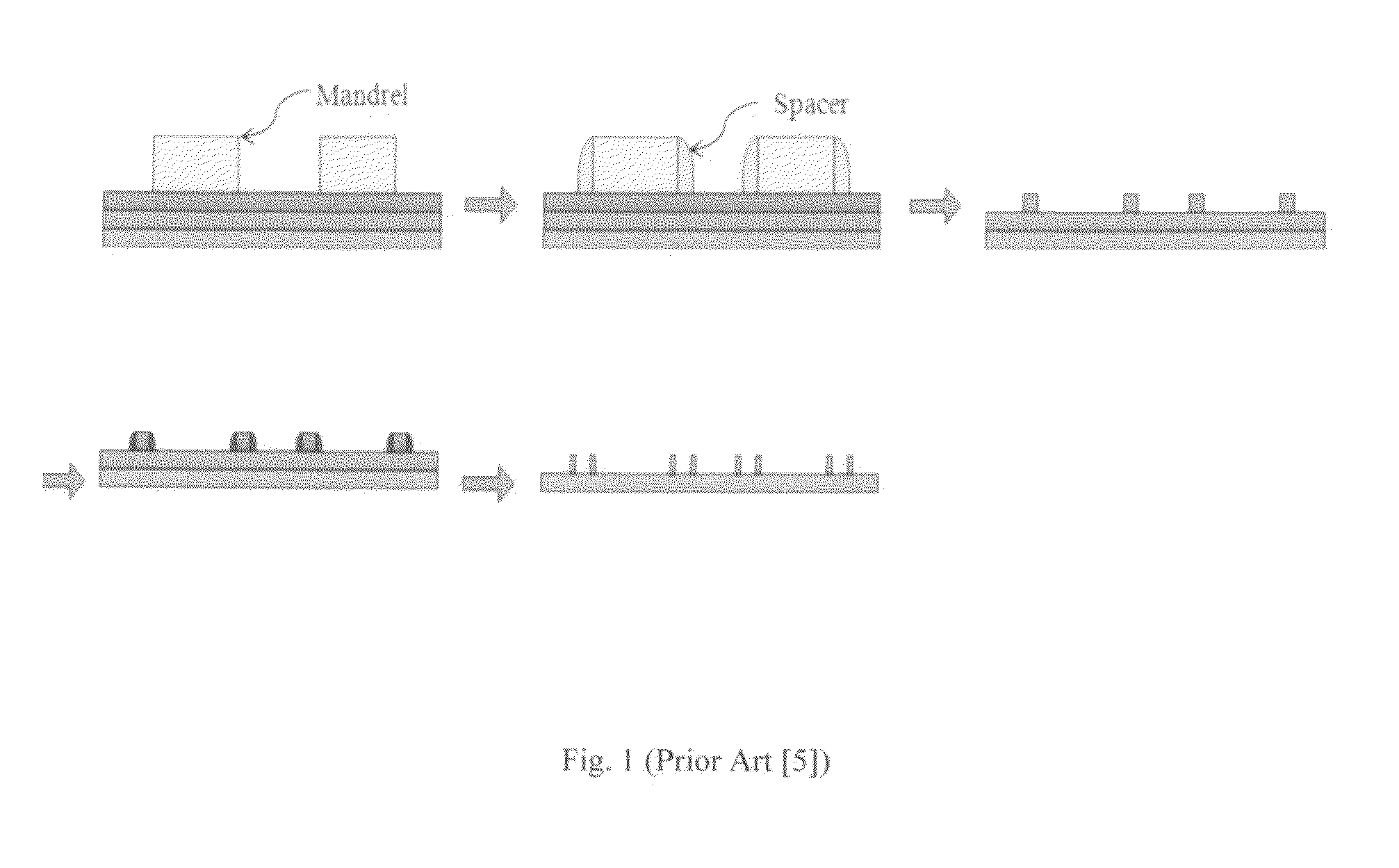
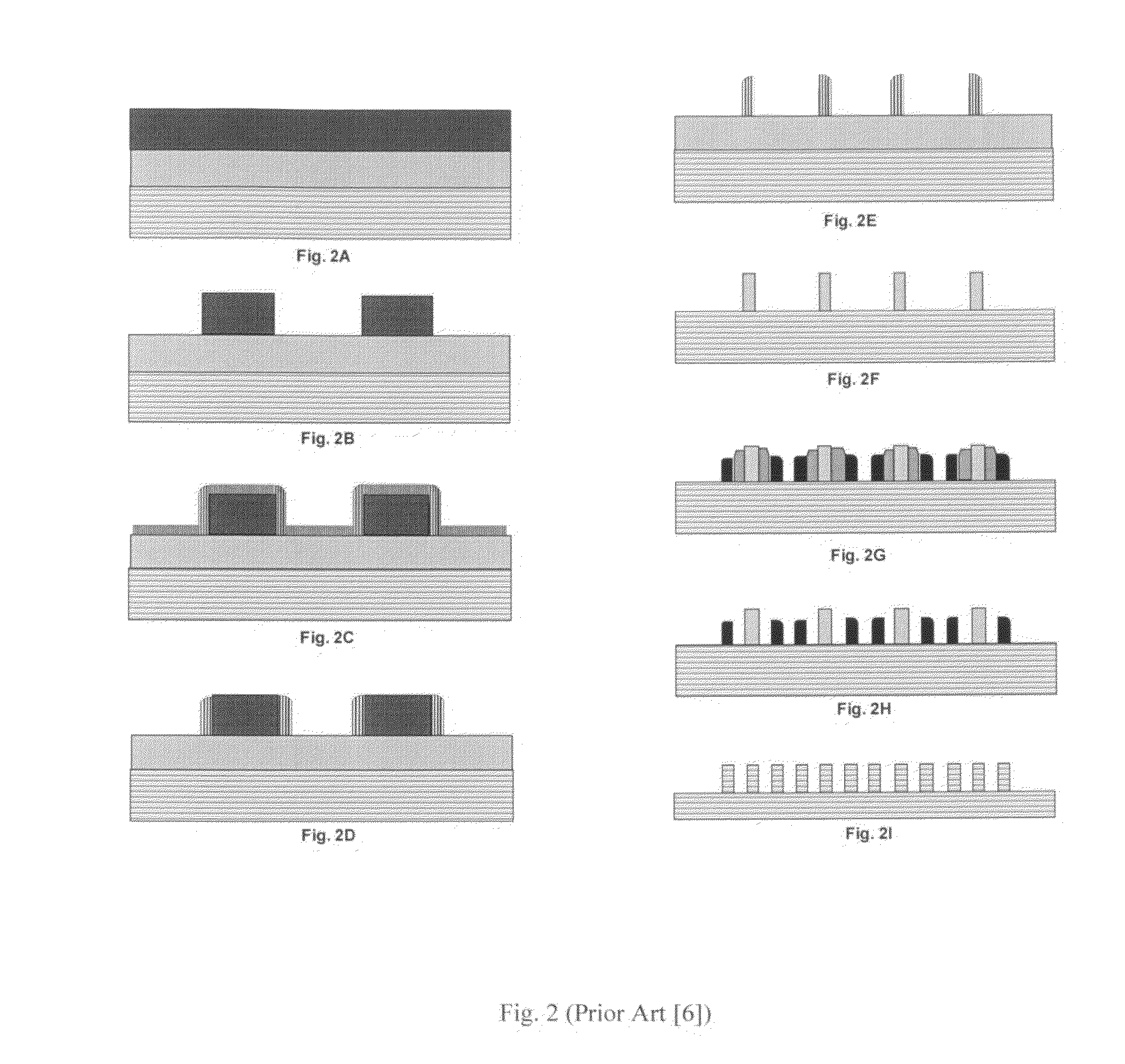
[0018]A number of novel layout decomposition and stitching techniques are developed in accordance with the invention. In one such process, random 2-D layout features are decomposed into two sets of features: one set of 1-D features arranged in one direction (defined to be X direction) and the other set of 1-D features arranged in the other direction (defined to be Y direction). In general, X and Y directions can be arbitrary and not necessarily orthogonal. These two sets of 1-D patterns are each separately formed by certain SAMP process (e.g., SAQP, SASP, or SAOP Process) using multiple masks (i.e., one mandrel mask and one / multiple cut masks). The type of SAMP process and the mask number to form the X-direction 1-D patterns, do not have to be the same as those to form Y-direction 1-D patterns.
[0019]To better understand and appreciate the invention, a flowchart is shown in FIG. 7 to depict the steps associated with a self-aligned quadruple patterning (SAQP) process according to one ...
PUM
 Abstract
Description
Claims
Application Information