Semiconductor device and method of manufacturing the same

a technology of semiconductor devices and semiconductor components, which is applied in the direction of resistors, semiconductor devices, diodes, etc., can solve the problems of reducing the reliability reducing the withstand voltage difficulty in improving so as to reduce the withstand voltage and improve the accuracy of the well resistance element. , the effect of high accuracy

Active Publication Date: 2016-02-18
RENESAS ELECTRONICS CORP
View PDF6 Cites 3 Cited by
  • Summary
  • Abstract
  • Description
  • Claims
  • Application Information

AI Technical Summary

Benefits of technology

[0011]According to an embodiment, it is possible to achieve high accuracy of a well resistance element by suppressing the dishing and stabilizing the resistance value of the well resistance element and to achieve suppression of decrease in withstand voltage due to electric field concentration of the well resistance element, so that it is possible to provide a semiconductor device including a well resistance element of high accuracy and high withstand voltage and a method of manufacturing the semiconductor device.

Problems solved by technology

Therefore, it is difficult to improve accuracy of the well resistance element.
Thereby, the current density in the well resistance element becomes partially uneven, so that there is a possibility that the electric current partially meanders or a partial concentration of electric field occurs and the withstand voltage of the well resistance element decreases.
This may reduce the reliability of the well resistance element that is expected to function as a high resistance element for high voltage.

Method used


Image

  • Semiconductor device and method of manufacturing the same
  • Semiconductor device and method of manufacturing the same
  • Semiconductor device and method of manufacturing the same

Examples


first embodiment

[0094]First, a semiconductor device in a wafer state will be described as an embodiment.

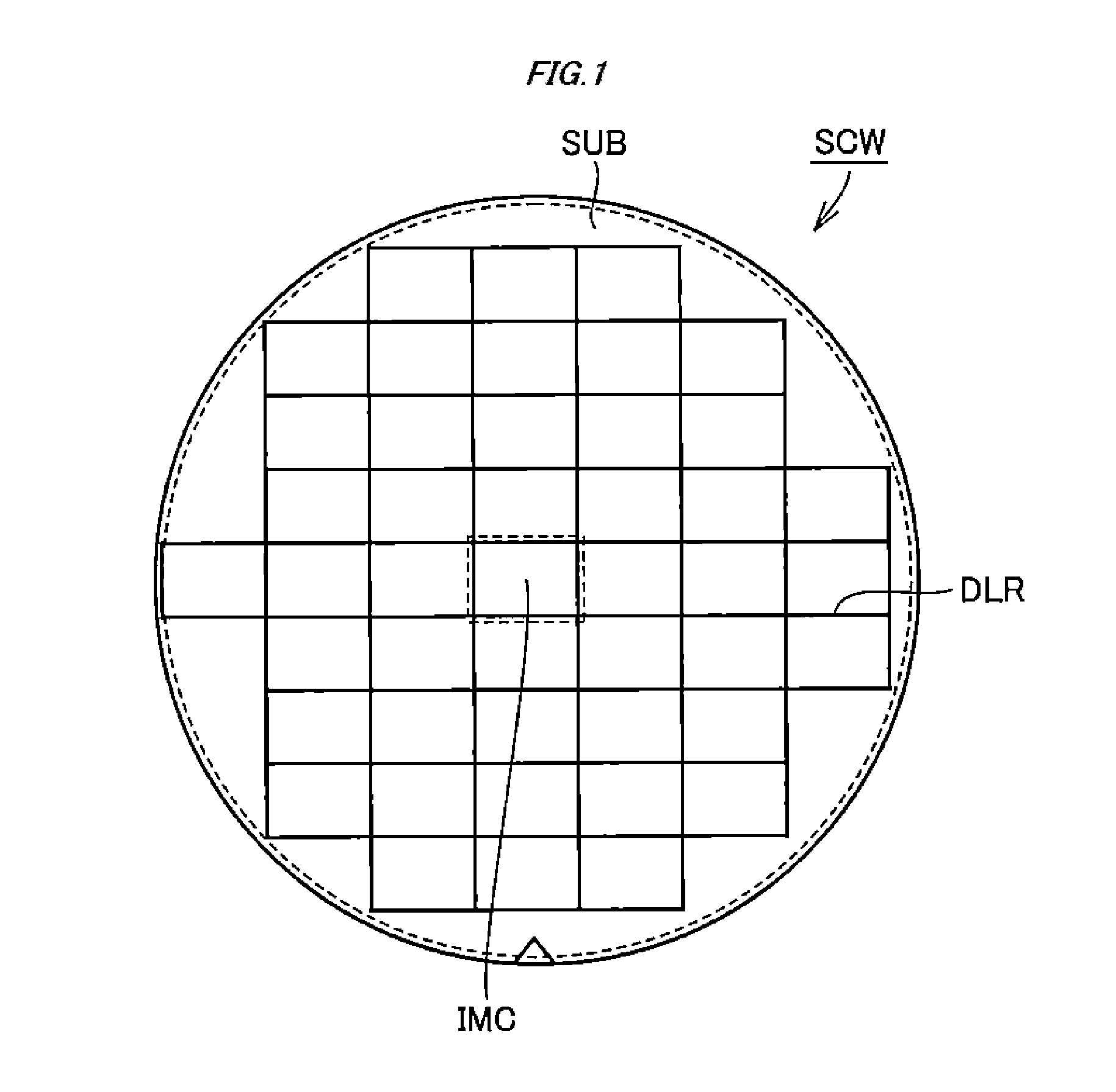
[0095]With reference to FIG. 1, a plurality of chip regions IMC of an solid state image sensing element is formed in a semiconductor wafer SCW formed of a semiconductor substrate SUB. Each of the chip regions IMC has a rectangular planar shape and the chip regions IMC are arranged in a matrix shape. In the semiconductor wafer SCW, a dicing line region DLR is formed between the chip regions IMC. The semiconductor wafer SCW is diced by the dicing line region DLR, so that the semiconductor wafer SCW is divided into a plurality of semiconductor chips.

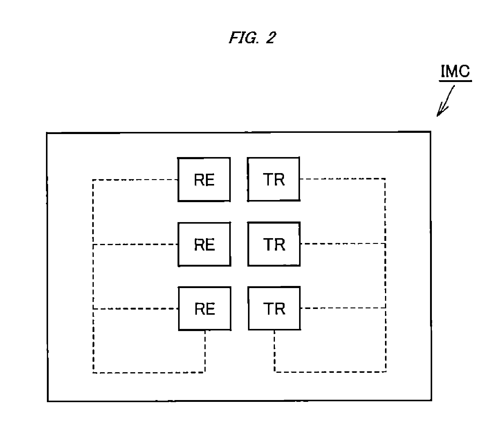
[0096]With reference to FIG. 2, in the chip region IMC that forms a divided semiconductor chip, for example, a resistance element region RE where a resistance element is arranged and a transistor region TR where a MOS (Metal Oxide Semiconductor) transistor used as a peripheral circuit is arranged are arranged. In FIG. 2, as an example, a plurality of res...

second embodiment

[0163]First, a well resistance element arranged in a resistance element region RE of the present embodiment will be described with reference to FIGS. 19 to 22.

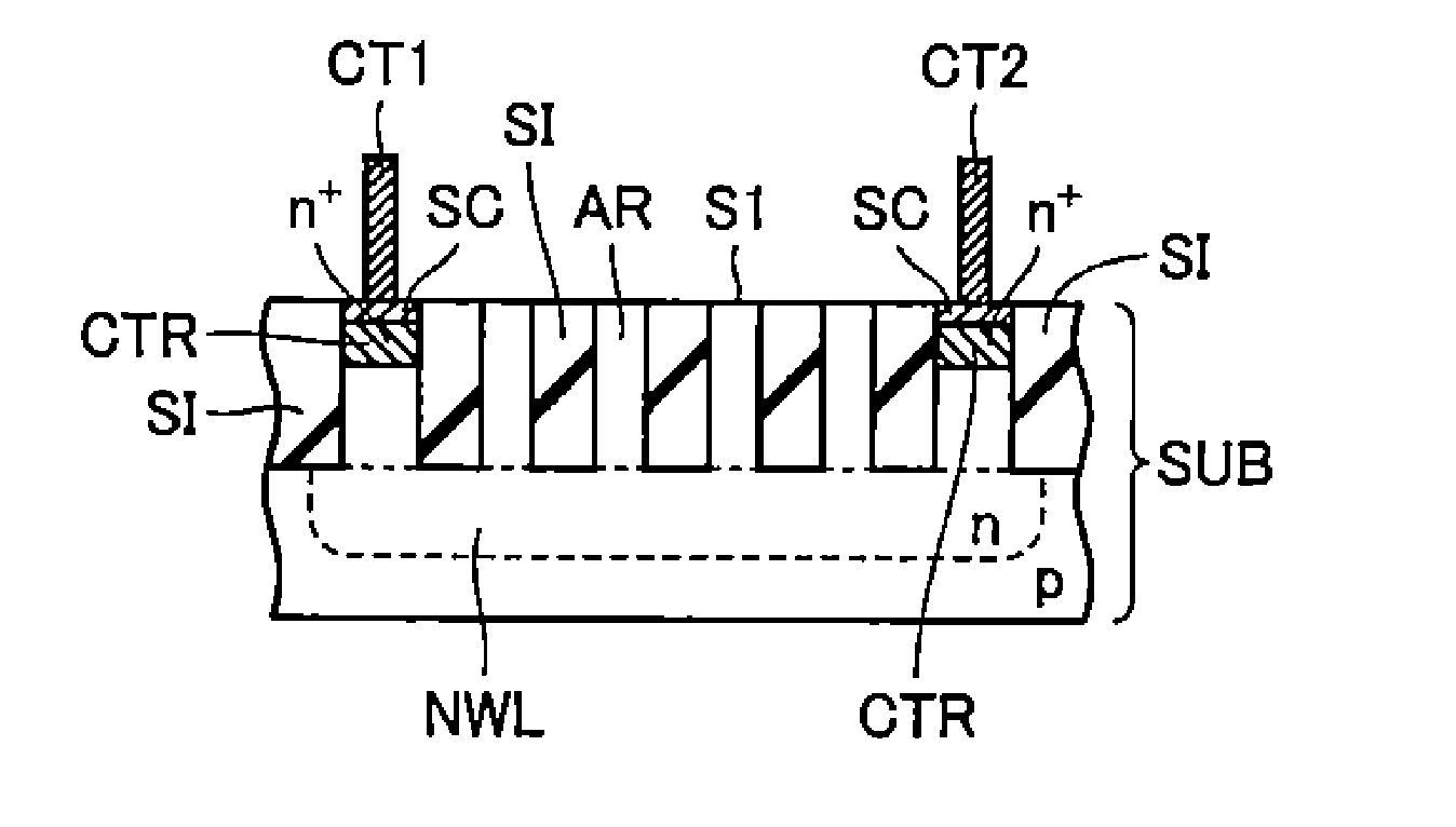
[0164]With reference to FIGS. 19 to 22, in the resistance element region RE of the present embodiment, a well resistance element is arranged, which is formed so that a p-type silicon semiconductor substrate SUB mainly includes the well region NWL, the contacts CT1 and CT2, the separation insulating films SI, and the active regions AR basically in the same manner as the well resistance element of the first embodiment. In the intermediate region between the input-side contact CT1 and the output-side contact CT2, the separation insulating film SI and the active regions AR, each of which has an elongated shape in plan view, are alternately and repeatedly arranged to be in contact with the upper surface of the well region NWL.

[0165]However, in the present embodiment, the separation insulating film SI and the active region AR in the...

third embodiment

[0183]First, a well resistance element arranged in a resistance element region RE of the present embodiment will be described with reference to FIGS. 27 to 30.

[0184]With reference to FIGS. 27 to 30, in the resistance element region RE of the present embodiment, a well resistance element that has basically the same configuration as that of the well resistance element of the second embodiment is formed. In other words, also in the present embodiment, the separation insulating film SI and the active region AR in the intermediate region extend in a direction (the vertical direction of FIG. 27) along the direction connecting the input-side contact CT1 and the output-side contact CT2 in plan view. Also in the present embodiment, a plurality of (here, five) input-side contacts CT1 and a plurality of (here, five) output-side contacts CT2 are arranged in the horizontal direction of FIG. 27 with a gap between them in plan view.

[0185]In the present embodiment, the separation insulating film SI...


PUM


Abstract

A semiconductor device including a well resistance element of high accuracy and high withstand voltage and a method of manufacturing the semiconductor device are provided.
The semiconductor device includes a semiconductor substrate, a well region, an input terminal, an output terminal, a separation insulating film, and an active region. The input terminal and the output terminal are electrically coupled to the well region. The separation insulating film is arranged to be in contact with the upper surface of the well region in an intermediate region between the input terminal and the output terminal. The active region is arranged to be in contact with the upper surface of the well region. The separation insulating film and the active region in the intermediate region have an elongated shape in plan view. In the intermediate region, a plurality of separation insulating films and a plurality of active regions are alternately and repeatedly arranged.

Description

CROSS-REFERENCE TO RELATED APPLICATION[0001]The disclosure of Japanese Patent Application No. 2014-164811 filed on Aug. 13, 2014 including the specification, drawings and abstract is incorporated herein by reference in its entirety.BACKGROUND[0002]The present invention relates to a semiconductor device and a method of manufacturing the same, and more particularly to a semiconductor device including a resistance element formed by a well region and a separation insulating film and a method of manufacturing the same.RELATED ART[0003]A resistance element, in particular, a well resistance element including a well region is used in many semiconductor integrated circuits as a high resistance element. For example, Japanese Patent Laid-Open No. 2008-21962 (Patent Literature 1) discloses a well resistance element having a structure in which a separation insulating film having a so-called STI (Shallow Trench Isolation) structure is formed on a main surface of a semiconductor substrate and a we...

Claims


Application Information

Patent Timeline
Patent Type & Authority Applications(United States)
IPC IPC(8): H01L29/06H01L21/311H01L21/762H01L21/8234H01L27/088H01L29/10H01L29/417
CPCH01L29/0653H01L29/1095H01L29/41758H01L29/0692H01L21/823418H01L21/823481H01L21/76224H01L21/823493H01L21/31144H01L27/088H01L27/0629H01L28/20H01L29/78
Inventor HAYASHI, KIYOSHI
Owner RENESAS ELECTRONICS CORP
Why Eureka
Try Eureka