Thin film transistor substrate and display using the same

a technology of thin film transistors and substrates, applied in static indicating devices, instruments, thermoelectric devices, etc., can solve problems such as limit on power consumption reduction, and achieve the effects of low power consumption, low off-current characteristics, and low frequency driving properties

Active Publication Date: 2016-03-03
LG DISPLAY CO LTD
View PDF3 Cites 53 Cited by
  • Summary
  • Abstract
  • Description
  • Claims
  • Application Information

AI Technical Summary

Benefits of technology

[0011]Another object of the present invention is to provide a thin film transistor substrate for a flat panel display having two different types of transistors manufactured by improved manufacturing processes and a reduced number of mask processes.
[0016]The thin film transistor substrate and a display using the same according to the present invention comprises two different types of thin film transistors on the same substrate, so that these two different types of thin film transistors can compensated for and complement each other. In particular, by including a thin film transistor having the low off-current characteristics, the display can have the low frequency driving property and the low power consumption property. Therefore, it is suitable for use in the portable and / or wearable appliances.

Problems solved by technology

However, with the conventional display technologies that have been developed to date, there are limitations on reducing power consumption.

Method used


Image

  • Thin film transistor substrate and display using the same
  • Thin film transistor substrate and display using the same
  • Thin film transistor substrate and display using the same

Examples


first example embodiment

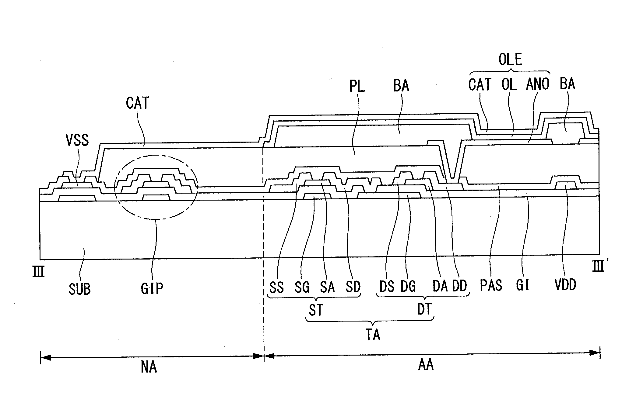
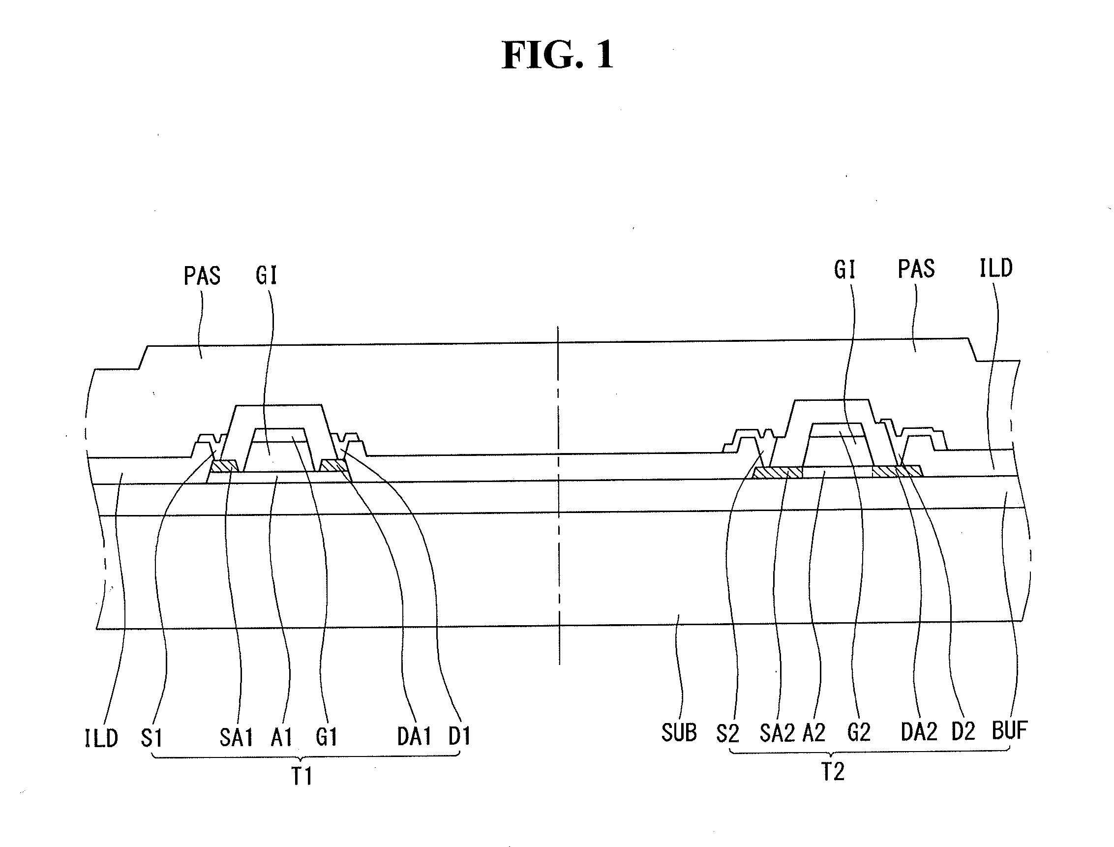
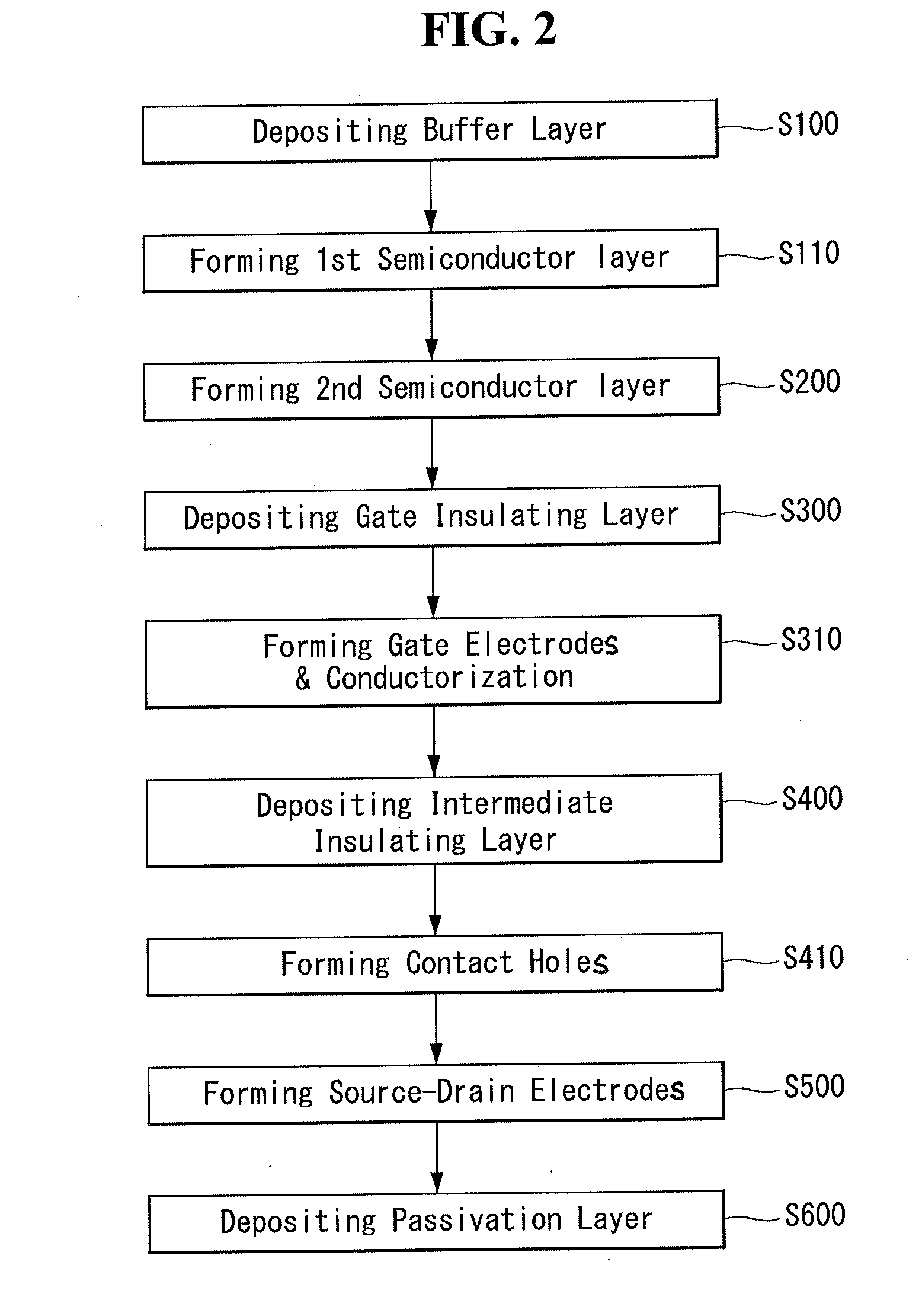
[0041]The first example embodiment of the present invention is discussed with reference to FIG. 1. FIG. 1 is a cross sectional view illustrating a structure of a thin film transistor substrate for a flat panel display in which two different types of thin film transistors are formed, according to the first example embodiment of the present invention. Here, the cross sectional views are more often referenced mainly because they more clearly show features of the example embodiments of the present invention than plane views.

[0042]As shown in FIG. 1, the thin film transistor substrate for a flat panel display according to the first example embodiment comprises a first thin film transistor T1 and a second thin film transistor T2, which are disposed on the same base substrate SUB. The base substrate SUB may hereinafter be referred to as the substrate SUB or the substrate. The first and second thin film transistors T1 and T2 may be disposed substantially far apart from each other, or they m...

second example embodiment

[0063]The second example embodiment of the present invention is discussed herebelow with reference to FIG. 3. FIG. 3 is a cross sectional view illustrating a structure of a thin film transistor substrate for a flat panel display in which two different types of thin film transistors are formed, according to the second example embodiment of the present invention.

[0064]In the first example embodiment, on the both side portions of the channel area in the polycrystalline semiconductor layer, the oxide semiconductor layer is formed and treated to become conductive to define the channel area. That is, the polycrystalline semiconductor layer does not have a doped area. Therefore, in some cases, there may be a potential issue of a relatively high resistance at the connection between the polycrystalline semiconductor layer and the source or drain electrode as it may lack an ohmic contact.

[0065]The second example embodiment provides a structure of the thin film transistor substrate having two ...

third example embodiment

[0092]Hereinafter, the third example embodiment of the present invention is discussed with reference to FIG. 5. FIG. 5 is a cross sectional view illustrating a structure of a thin film transistor substrate for a flat panel display in which two different types of thin film transistors are formed, according to the third example embodiment of the present invention.

[0093]With respect to the features of the structure and the manufacturing process, the third example embodiment is very similar to the first example embodiment. The differences may include how a channel area is defined. For example, the channel area may be defined by a process to make the channel area conductive in the first example embodiment, whereas the channel area may be defined by a doping process in the third example embodiment. The third example embodiment may be more suitable for manufacturing the two different types of thin film transistors that are directly and / or serially connected to each other on the same substr...


PUM


Abstract

The present invention relates to a thin film transistor substrate having two different types of semiconductor materials on the same substrate, and a display using the same. A disclosed display may include a substrate, a first thin film transistor having a polycrystalline semiconductor material on the substrate and a second thin film transistor having an oxide semiconductor material on the substrate.

Description

[0001]This application claims the benefit of Korea Patent Application Nos. 10-2014-0114302 filed on Aug. 29, 2014, 10-2014-0114305 filed on Aug. 29, 2014, 10-2014-0114307 filed on Aug. 29, 2014, and 10-2015-0113281 filed on Aug. 11, 2015, and the U.S. Provisional Patent Application Nos. 62 / 043,449 field on Aug. 29, 2014, 62 / 043,447 field on Aug. 29, 2014, and 62 / 043,470 filed on Aug. 29, 2014, which are each incorporated herein by reference for all purposes as if fully set forth herein.BACKGROUND OF THE INVENTION[0002]1. Field of the Invention[0003]The present invention relates to a thin film transistor substrate, and more particularly, to a thin film transistor substrate having two different types of semiconductor materials on the same substrate, and a display using the same.[0004]2. Discussion of the Related Art[0005]As the information society continues to develop, displays for depicting information are increasingly required in various ways to do more. Accordingly, various flat pa...

Claims


Application Information

Patent Timeline
Patent Type & Authority Applications(United States)
IPC IPC(8): H01L27/32G09G3/32H01L27/12H01L29/786
CPCH01L27/3262H01L29/7869H01L29/78675H01L27/1222H01L27/124G09G2310/0297G09G3/3225G09G3/3275G09G2300/0426G09G2330/028G09G2330/021H01L27/3276H01L27/1214H01L27/1251H10K59/1213H01L27/1225H01L29/78696
Inventor OH, SAEROONTERLEEBAECK, JUHEYUCKKWON, HOIYONGJEON, JEYONGLEE, DOHYUNG
Owner LG DISPLAY CO LTD
Why Eureka
Try Eureka