Spin wave device and logic circuit using spin wave device

a logic circuit and spin wave technology, applied in the direction of power consumption reduction, pulse technique, instruments, etc., can solve the problems of processing limits and power consumption reduction, and achieve the effects of low power consumption, high speed, and miniaturization

Inactive Publication Date: 2016-04-14
HITACHI LTD
View PDF7 Cites 8 Cited by
  • Summary
  • Abstract
  • Description
  • Claims
  • Application Information

AI Technical Summary

Benefits of technology

[0013]By applying the logic circuit using the spin wave, it is possible to realize ultra-low power consumption, miniaturization, and high speed that cannot be realized by the conventional logic circuit using the CMOS.

Problems solved by technology

However, a logic integrated circuit that takes on the analysis and the processing has limits in a reduction in power consumption through element refining of a conventional COMS and operation optimization.

Method used


Image

  • Spin wave device and logic circuit using spin wave device
  • Spin wave device and logic circuit using spin wave device
  • Spin wave device and logic circuit using spin wave device

Examples


first embodiment

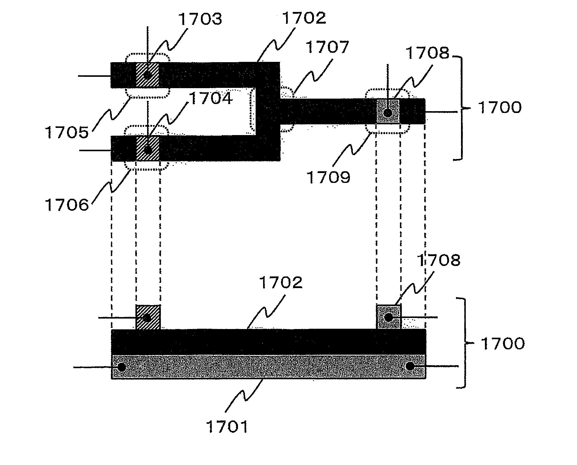
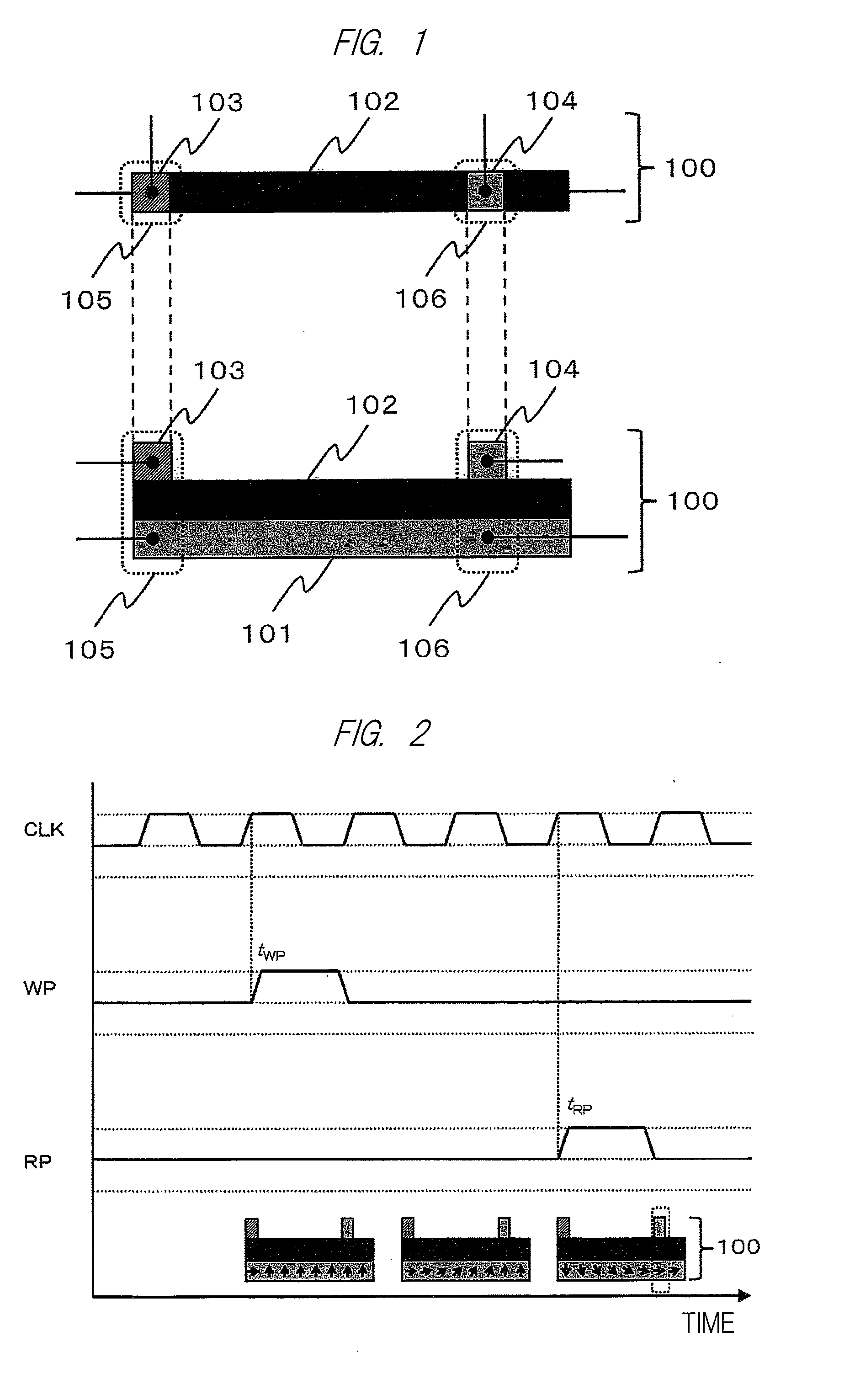
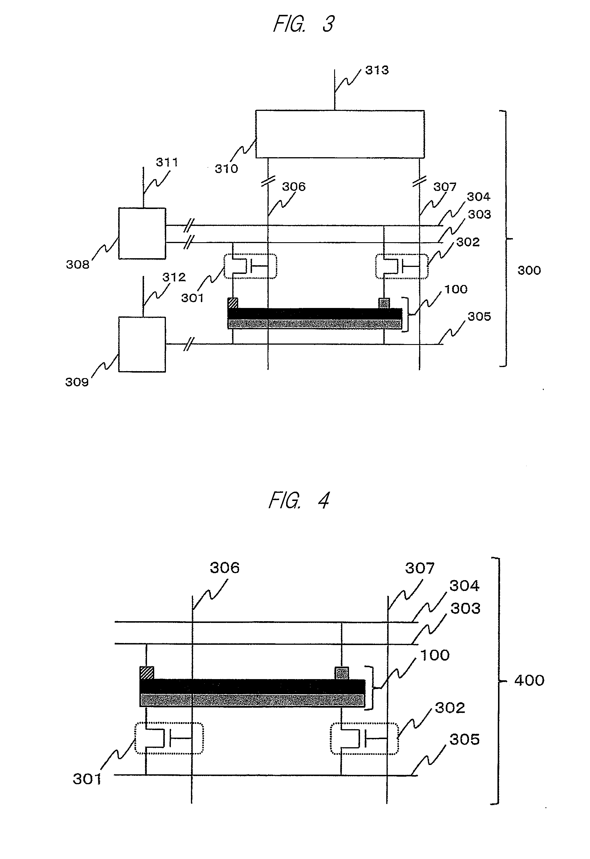
[0034]A spin wave device is a device that converts an input signal (“0” or “1”) into a spin wave corresponding to “0” or “1”, propagates the spin wave to an output unit present in a place apart from an input unit, and read out. Major characteristics are that consumption of electric power is extremely small in a portion that generates the spin wave corresponding to the input signal, a portion that propagates the spin wave, and a portion that outputs the spin wave. It is possible to convert two input signals respectively into spin waves, cause the two spin waves to interfere with each other to cause the spin waves to operate like a logic gate, and output logic. By disposing the logic gate by the spin wave device in multiple stages, it is possible to form a logic circuit. In the following explanation, an operation principle of the spin wave device is explained with reference to the figures.

[0035]According to a viewpoint of the invention, as shown in FIG. 1, a spin wave device 100 inclu...

second embodiment

[0056]In the spin wave device 100 described in the first embodiment, the spin wave having the information of “1” is the wave approximately π / 2 different in the phase from the spin wave having the information of “0”. According to another viewpoint of the invention, the spin wave having the information of “1” may be a wave phase-shifted by π from the spin wave having the information “0”. A basic structure of the spin wave device 100 described in a second embodiment is the same as the basic structure shown in FIG. 1. Operation timings of a clock signal, a WP applied from the first electrode 103, and an RP applied from the second electrode 104 are basically the same as the operation timings in FIG. 5. FIG. 8 is a diagram showing a temporal change of an output signal obtained by measuring, via a reference resistor, as a voltage, the magnitude of an output current at the time when a micro-voltage is applied in the film surface perpendicular direction of the output portion 106. In an outpu...

third embodiment

[0057]In the spin wave device 100 described in the first embodiment and the second embodiment, the information of “0” or “1” of the spin wave is characterized by the phase of the spin wave. According to another viewpoint of the invention, information of “0” or “1” of the spin wave can be characterized by the amplitude of the spin wave. FIG. 9 is schematically shows a spin wave having information of “0” and “1” propagated to the output portion 106 and a magnetization direction of the first ferromagnetic layer 101 at that point. In an example shown in FIG. 9, the amplitude of the spin wave having the information of “0” is plus. At t1, a magnetization direction of a portion of the first ferromagnetic layer 101 included in the output portion 106 is a parallel rightward direction with respect to a film surface. On the other hand, the amplitude of the spin wave having the information of “1” is minus. At t1, the magnetization direction of a portion of the first ferromagnetic layer 101 incl...


PUM


Abstract

As a technique for attaining a reduction in power consumption, there is a technique for reducing power consumption using a spin wave. No specific proposal concerning spin wave generation, spin wave detection, and a latch technique for information has been made.A device applies an electric field to a first electrode of a nonmagnetic material using a thin line-shaped stacked body including a first ferromagnetic layer and a nonmagnetic layer to thereby generate a spin wave in the first ferromagnetic layer, and detects a phase or amplitude of the spin wave propagated in the first ferromagnetic layer using a second electrode of a ferromagnetic material with a magnetoresistance effect.

Description

TECHNICAL FIELD[0001]The present invention relates to a spin wave device including spin wave generation, spin wave propagation, spin wave detection, and a latch technique for information and further relates to an ultra-low power consumption logic integrated circuit using the spin wave device.BACKGROUND ART[0002]It is said that a reduction in power consumption in an LSI for a trunk network router is essential to cope with a global increase in an amount of information communication. There are increasing needs for analyzing and processing, at high speed and low costs, a large amount of indefinite dynamic data accumulated in a server. However, a logic integrated circuit that takes on the analysis and the processing has limits in a reduction in power consumption through element refining of a conventional COMS and operation optimization.[0003]As means for solving these problems, there is a method of using a spin wave described in NPL 1. The spin wave means spatial and temporal changes in ...

Claims


Application Information

Patent Timeline
Patent Type & Authority Applications(United States)
IPC IPC(8): H03K19/00H01L43/02H03K3/356H03L7/00H03K19/18H01L43/08H01L27/22
CPCH03K19/0016H01L43/08H01L43/02H03K3/356H03L7/00H03K19/18H01L27/22H01L29/82H03K19/16H01L29/66984H01L29/1029G11C11/161G11C11/1675G11C11/1659G11C11/14G11C11/1673G11C11/1693H10B61/00H10N59/00H10N50/10H10N50/80
Inventor MIURA, KATSUYAOGAWA, SUSUMUITO, KENCHIYAMADA, MASAKI
Owner HITACHI LTD
Why Eureka
Try Eureka