Single-chip bridge-type magnetic field sensor

a magnetic field sensor and single-chip technology, applied in the field of magnetic field sensors, can solve the problems of low cost mass production of gmr or tmr sensors, two films are less consistent, and the process is complicated, so as to achieve good linearity, high sensitivity, and good linearity

Active Publication Date: 2016-04-21
MULTIDIMENSION TECH CO LTD
View PDF3 Cites 10 Cited by
  • Summary
  • Abstract
  • Description
  • Claims
  • Application Information

AI Technical Summary

Benefits of technology

[0045](1) The reference arm and the sense arm magnetoresistive elements have the same pinned layer direction, so that it is not necessary to use two different thin films or a local annealing process in order to yield a single-chip sensor.
[0046](2) Through the use of the elongated shield structure, the sensor can achieve good linearity and high s...

Problems solved by technology

Although both GMR and TMR are compatible with standard semiconductor manufacturing processes, high sensitivity GMR or TMR sensors have yet not begun low cost mass production.
The production yield of GMR and TMR magnetoresistive sensors depends on the achievable offset value, and this is difficult when forming a bridge utilizing GMR or TMR magnetoresistive elements.
In the two film process, the two respective TMR pinned layers are set in opposite directions; it makes the process complicated, because it requires a second annealing that affects the layer that was deposited first, the makes the matching of the two films less consistent, which affects the overall performance of the sensor.
Unfortunately, this method requires custom equipment, which is expensive to develop, and the local laser annealing process is slow.
Unfortunately, this method leads to smaller dynamic range of the sensor response, reducing the operating range.
(3) using magnetic shielding to provide flux concentrators in referenced bridge sensors, in the present art this method results...

Method used


Image

  • Single-chip bridge-type magnetic field sensor
  • Single-chip bridge-type magnetic field sensor
  • Single-chip bridge-type magnetic field sensor

Examples


example 1

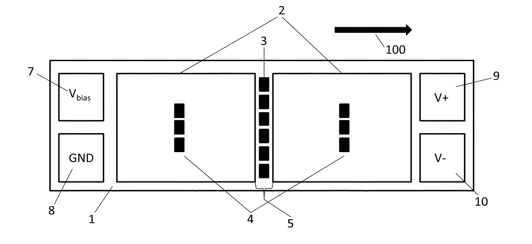
[0061]FIG. 2 shows a schematic diagram of a single-chip full-bridge magnetic field sensor of the present invention. The sensor comprises a substrate 1, a Wheatstone full-bridge deposited on the substrate 1, eight shielding structures 42 and four pads 7-10. The first bridge comprises reference arm R1 and sense arm S1, while the second bridge arm comprises reference arm R2 and sense arm S2; the reference arms R1 and R2 include three reference element strings each respectively, three in the first reference arm, and three in the second reference arm; the sense arms S1 and S2 include three sense element strings each respectively, three in the first sense arm, and three in the second sense arm. Each reference element string and each sensor element string are composed of one or more identical magnetoresistive sense elements that are electrically interconnected. As shown in FIG. 2, reference arm R1 and sense arm S1, reference arm R2 and sense arm S2 are composed of six identical magnetoresi...

example 2

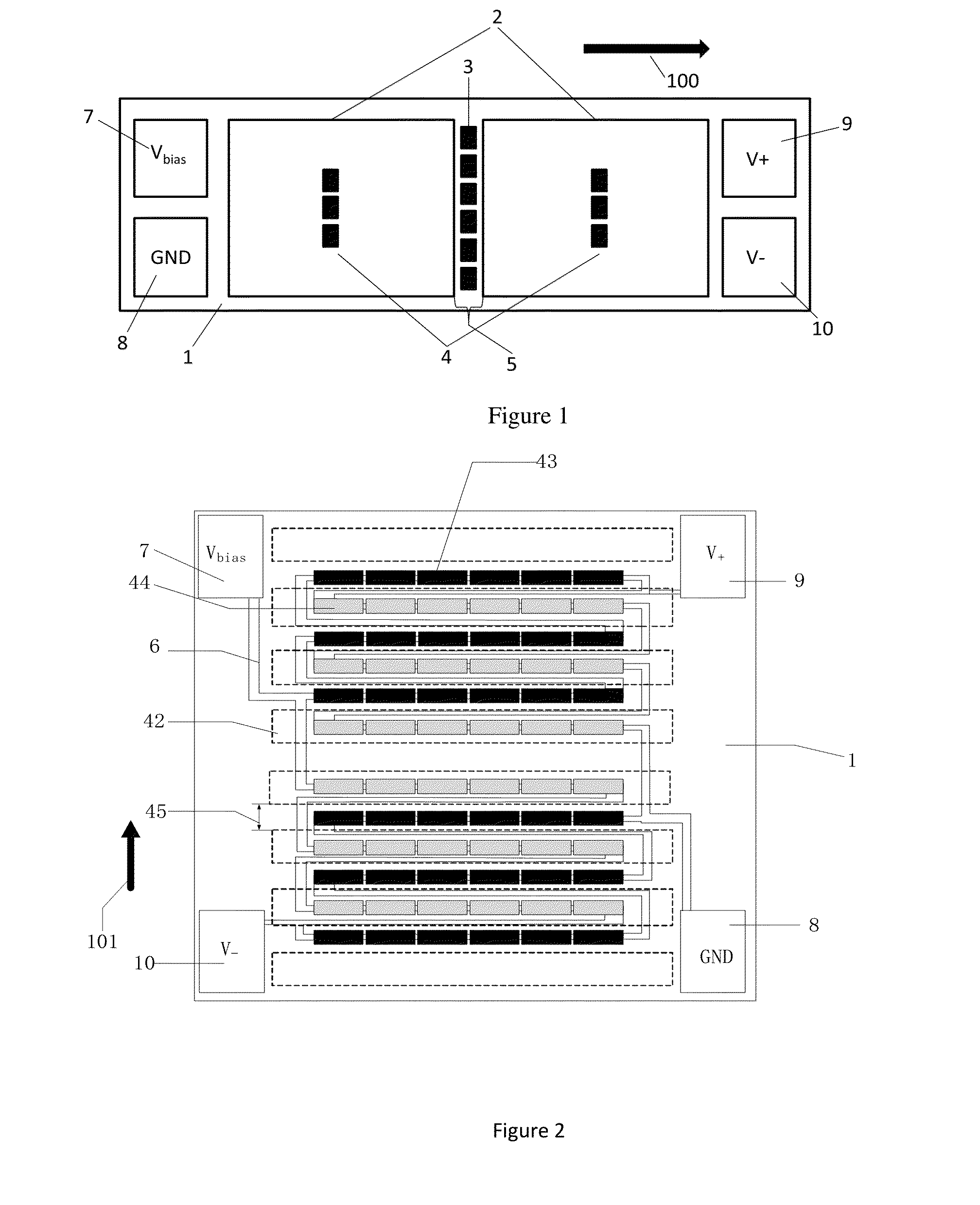
[0069]FIG. 12 shows another implementation of the present invention. The sensor consists of a substrate 1, and onto the substrate a Wheatstone half-bridge is deposited, it has 6 shielding structures 42, and three wire bond pads 7-9. The Wheatstone half-bridge includes a reference arm R1 and a sense arm S1, each individually including 3 horizontal reference element strings 44 and 3 horizontal sense element strings 43, each reference element string 44 and each sense element string 43 includes a multitude of identical magnetoresistive sensing elements electrically interconnected, and there are 6 magnetoresistive elements per string shown in the figure. The sense element strings 43 and the reference element strings 44 are spaced vertically with respect to each other, and the spacing between the adjacent reference element strings 44 and sense element strings is L. The adjacent shielding structures 42 have a gap 45 between them, where the length and width of the gap 45 are different. Each...

example 3

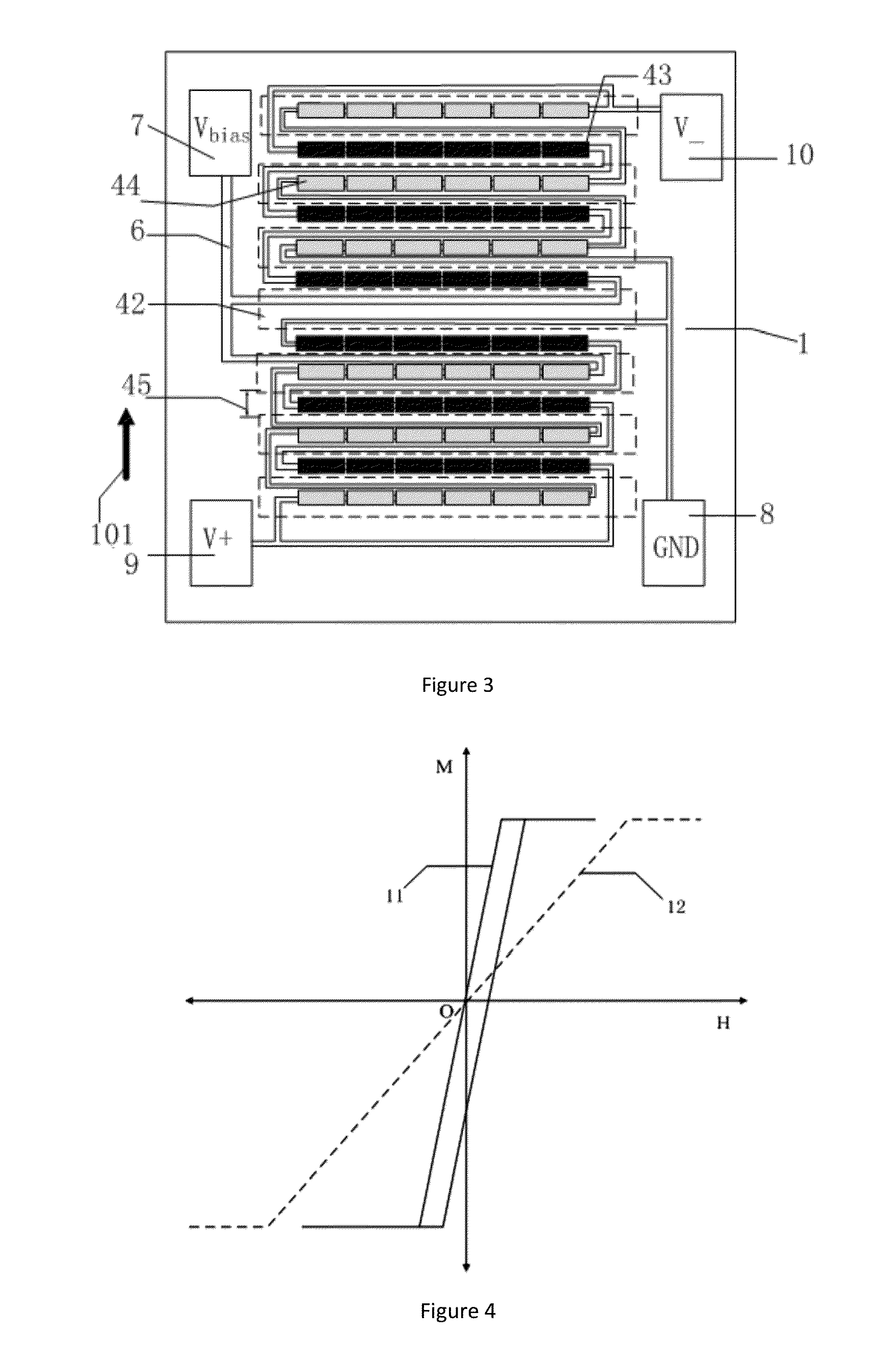
[0072]The difference between this example and the second example is the use of a quasi Wheatstone bridge circuit. This single-chip magnetic field sensor bridge contains three wire bond pads, and of the three wire bond pads the first is used for grounding, while the second wire bond pad and the third wire bond pads are used for signal outputs. The Wheatstone quasi-bridge includes two identical current sources I1 and I2, a reference arm R1, and a sense arm S1. The current sources I1 and I2, the reference arm R1 and the sense arm S1 each have a first end and a second end. The first wire bond pad is electrically connected with the first end of reference arm R1, the first end of sense arm S1, and the first end of the two current sources I1 and I2. The second wire bond pad is electrically connected with the second end of reference are R1 and the second end of current source I2. The third wire bond pad is electrically connected with the second end of sense arm S1 and with the second end of...


PUM


Abstract

A single-chip magnetic field sensor bridge, comprising a substrate, a reference arm, a sensing arm, shielding structures, and wire bond pads is disclosed. The reference arm and the sense arm respectively comprise at least two rows/columns of reference element strings and sense element strings formed by electrically connecting one or more identical magnetoresistive sensing elements. The reference element strings and the sense element strings are alternately arranged. The magnetoresistive sensing elements are AMR, GMR or TMR sensing elements. The reference element strings are provided with shielding structures thereon, and the sensing element strings are located in gaps between two adjacent shielding structures. The shielding structures are arrays of elongated strips composed of permalloy or another soft ferromagnetic material. The sensors can be implemented as one of three different bridge structures, called a quasi-bridge, a half-bridge, or a full-bridge. This single-chip magnetic field sensor bridge has the advantages of small size, low cost, high sensitivity, small offset, good linearity, and good temperature stability.

Description

TECHNICAL FIELD[0001]The invention relates to magnetic sensor technology especially that involving a single-chip magnetic field sensor bridge with low offset.BACKGROUND TECHNOLOGY[0002]TMR (tunneling magnetoresistance) sensors are a new magnetoresistive sensing technology that is beginning to find use in industrial applications. This sensor technology uses tunneling magnetoresistive multilayer thin film materials for sensing the magnetic field, and the main features are: the magnetic multilayer film produces a big change in resistance in response to a change in magnitude or direction of the external magnetic field. Compared to other practical applications utilizing the AMR effect (anisotropic magnetoresistance) of the GMR effect (giant magnetoresistance), the rate of change of resistance is much greater, and additionally compared to the Hall Effect it has much better temperature stability.[0003]Although both GMR and TMR are compatible with standard semiconductor manufacturing proces...

Claims


Application Information

Patent Timeline
IPC IPC(8): G01R33/09G01R17/10
CPCG01R17/105G01R33/09
Inventor DEAK, JAMES GEZA
Owner MULTIDIMENSION TECH CO LTD
Why Eureka
Try Eureka