Method for Reducing Contact Resistance in MOS

Active Publication Date: 2016-05-19
INTERUNIVERSITAIR MICRO ELECTRONICS CENT (IMEC VZW)
View PDF12 Cites 8 Cited by
  • Summary
  • Abstract
  • Description
  • Claims
  • Application Information

AI Technical Summary

Benefits of technology

[0039]In embodiments, the doped region may be from 1 to 10 nm deep. This is advantageous because it creates less stress in the surface and it minimizes short channel behaviour.
[0040]In embodiments, the doped region may be conformal. This is advantageous as it promotes homogeneous growth of the nucleation layer.
[0041]In embodiments, the doping range of the doped region may be from 1018 to 5×1019 cm−3, preferably from 1018 to 1019 cm−3. It has surprisingly been found that a doping level within such a relatively low doping range (a typical doping range of the prior art is 1020-1021 cm−3) is sufficient to achieve low contact resistivity (below 10−8 Ω·μm2) for the

Problems solved by technology

This in turn leads to a disappointingly high contact resi

Method used


Image

  • Method for Reducing Contact Resistance in MOS
  • Method for Reducing Contact Resistance in MOS
  • Method for Reducing Contact Resistance in MOS

Examples


example 1

Manufacture of a Si Fin Comprising an Area on which a InAs Source (or Drain) Structure Will be Grown

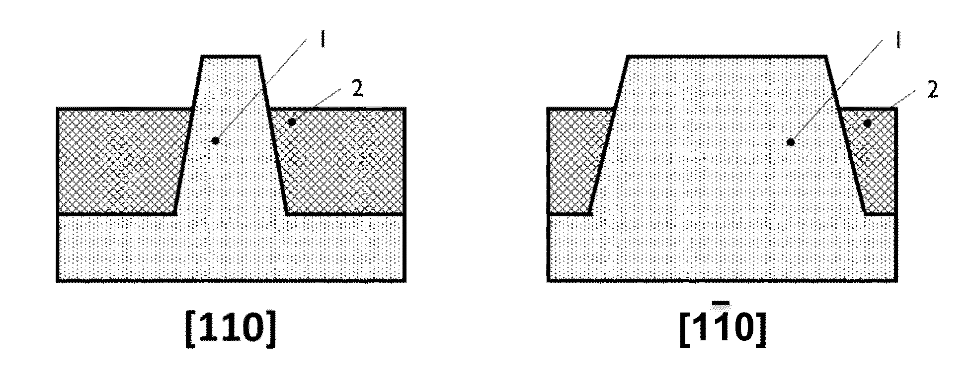
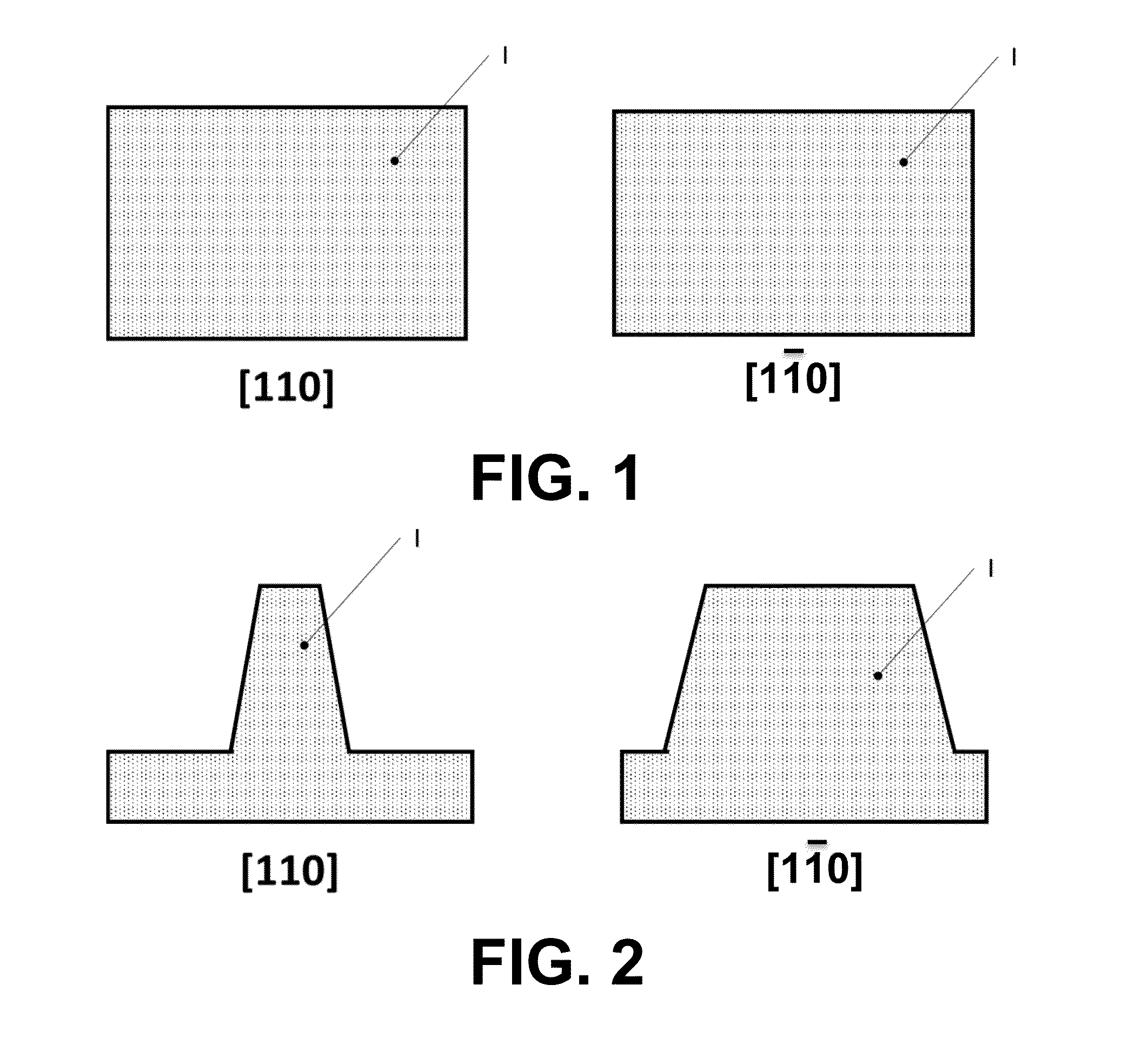
[0076]FIG. 1 shows the silicon substrate (1) before formation of the fin. The left side of FIG. 1 shows a cross-section of the substrate (1) perpendicular to the [110] direction. The right side of FIG. 1 shows a cross-section of the substrate (1) perpendicular to the [110] direction which is itself perpendicular to the [110] direction. In the following, the cross-section of the substrate perpendicular to the [110] direction will be referred to as the front cross-sectional view while the cross-section of the substrate perpendicular to the [110] direction will be referred to as the side cross-sectional view.

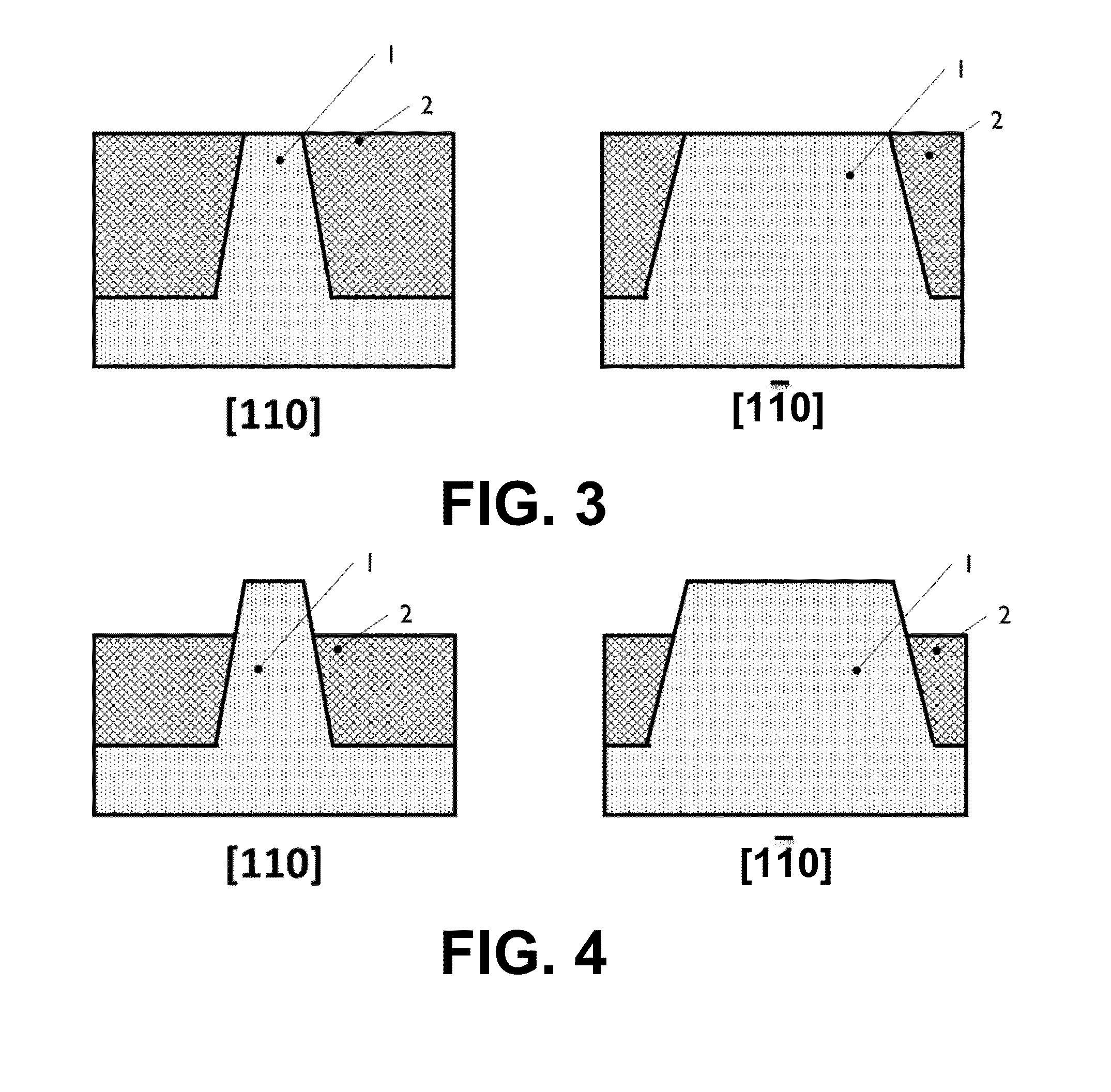
[0077]FIG. 2 shows the fin obtained after an etching process operated on the silicon substrate (1). Both cross-sections are cutting in half the area of the substrate where the InAs structure will be grown.

[0078]FIG. 3 shows the formation of a shallow trench isolation (STI) by filling...

example 2

Growing of a InAs Source (or Drain) Structure on the Structure of Example 1

[0081]The sample of Example 1 was placed in a MOVPE (MetalOrganic Vapor Phase Epitaxy) reactor.

[0082]Referring now to FIG. 6, prior to the InAs selective area growth, the surface of the fin was thermally cleaned from its native oxide by heating it up to a temperature of 850° C. under a H2 atmosphere at a pressure of less than 100 mbar for a period of from 5 to 10 min. If the substrate is made of Ge instead of Si, the backing should be performed above 500° C. For an intermediate composition of the substrate (SinGe1-n), an intermediate temperature is suitable and can be easily determined by trial and errors.

[0083]Following this bake step, the temperature was kept at the same bake temperature with pressure between 50 mbar and 500 mbar during 15 min to expose the Si surface to tertiarybutylarsine in order to promote the interdiffusion of As into a top portion of the Si fin. Alternatively, AsH3 could also have bee...

example 3

Growing of a InAs Layer on a Pre-Formed Source (or Drain) Structure

[0086]By a process analog to the one described in Example 2, an InAs (or other III-V) layer can be grown on top of a pre-formed SinGe1-n source or drain. For this purpose, the same process of Example 2 can be repeated except that it starts by cleaning the surface of the pre-formed SinGe1-n source or drain instead of cleaning the fin. It then proceeds by exposing the source or drain surface to an As precursor, exposing the source or drain at a lower temperature to tertiarybutylarsine and trimethylindium until a thickness of InAs of about 5-10 nm is obtained, and growing a layer of InAs at a higher temperature until the desired height is obtained. In this case, InAs is used to reduce the contact resistance of the pre-existing source / drain.


PUM


Abstract

A method for growing a III-V semiconductor structure on a SinGe1-n substrate, wherein n is from 0 to 1 is provided. The method includes the steps of: (a) bringing a SinGe1-n substrate to a high temperature; (b) exposing the area to a group V precursor in a carrier gas for from 5 to 30 min, thereby forming a doped region at said area; (c) bringing the SinGe1-n substrate to a low temperature; (d) exposing the doped region to a group III precursor in a carrier gas and to a group V precursor in a carrier gas until a nucleation layer of III-V material of from 5 to 15 nm is formed on the nucleation layer; (e) bringing the SinGe1-n substrate to an intermediate temperature; and (f) exposing the nucleation layer to a group III precursor in a carrier gas and to a group V precursor in a carrier gas.

Description

TECHNICAL FIELD OF THE INVENTION[0001]The present invention relates to the field of semiconductor devices and their construction. In particular it relates to a method for reducing contact resistance in transistors.BACKGROUND OF THE INVENTION[0002]In order to enable a higher component density on integrated circuits, much effort is invested in decreasing the size of these components.[0003]Currently, industry is striving to reach the 10 nm technology node. In this node, the gate length in transistors may be smaller than 20 nm. Components currently envisioned for this technology node such as Si FinFET and high mobility channel devices need to fulfil stringent requirements concerning their external resistance.[0004]According to the ITRS roadmap edition 2012, the external resistance of these devices will need to be reduced to less than 100 Ωμm for Ge / III-V and less than 180 Ωμm for Si.[0005]A large part of the resistance is coming from the contact resistance (contact plug or local interco...

Claims


Application Information

Patent Timeline
IPC IPC(8): H01L29/66H01L29/417H01L29/78H01L29/20
CPCH01L29/66795H01L29/7848H01L29/41725H01L29/20H01L21/02381H01L21/0243H01L21/02455H01L21/02546H01L21/02549H01L21/0262H01L21/02639H01L21/02658H01L21/02661H01L21/76224H01L29/0847H01L29/267H01L29/7851H01L21/02387H01L21/02392H01L21/02395H01L21/02513
Inventor MERCKLING, CLEMENTCOLLAERT, NADINE
Owner INTERUNIVERSITAIR MICRO ELECTRONICS CENT (IMEC VZW)
Why Eureka
Try Eureka