Semiconductor device

Active Publication Date: 2016-05-26
SEMICON ENERGY LAB CO LTD
View PDF9 Cites 4 Cited by
  • Summary
  • Abstract
  • Description
  • Claims
  • Application Information

AI Technical Summary

Benefits of technology

[0020]An object of one embodiment of the present invention is to provide a semiconductor device including a transistor with low off-state current. Another object of one embodiment of the present invention is to provide a semiconductor device with low power consumption. Another object of one embodiment of the present invention is to provide a miniaturized semiconductor device. Another object of one embodiment of the present invention is to provide a highly reliable semiconductor device. Another object of one embodiment of the present invention is to provide a semiconductor device capable of high-speed wri

Problems solved by technology

For example, a display device for which a transistor including an

Method used


Image

  • Semiconductor device
  • Semiconductor device
  • Semiconductor device

Examples


embodiment 1

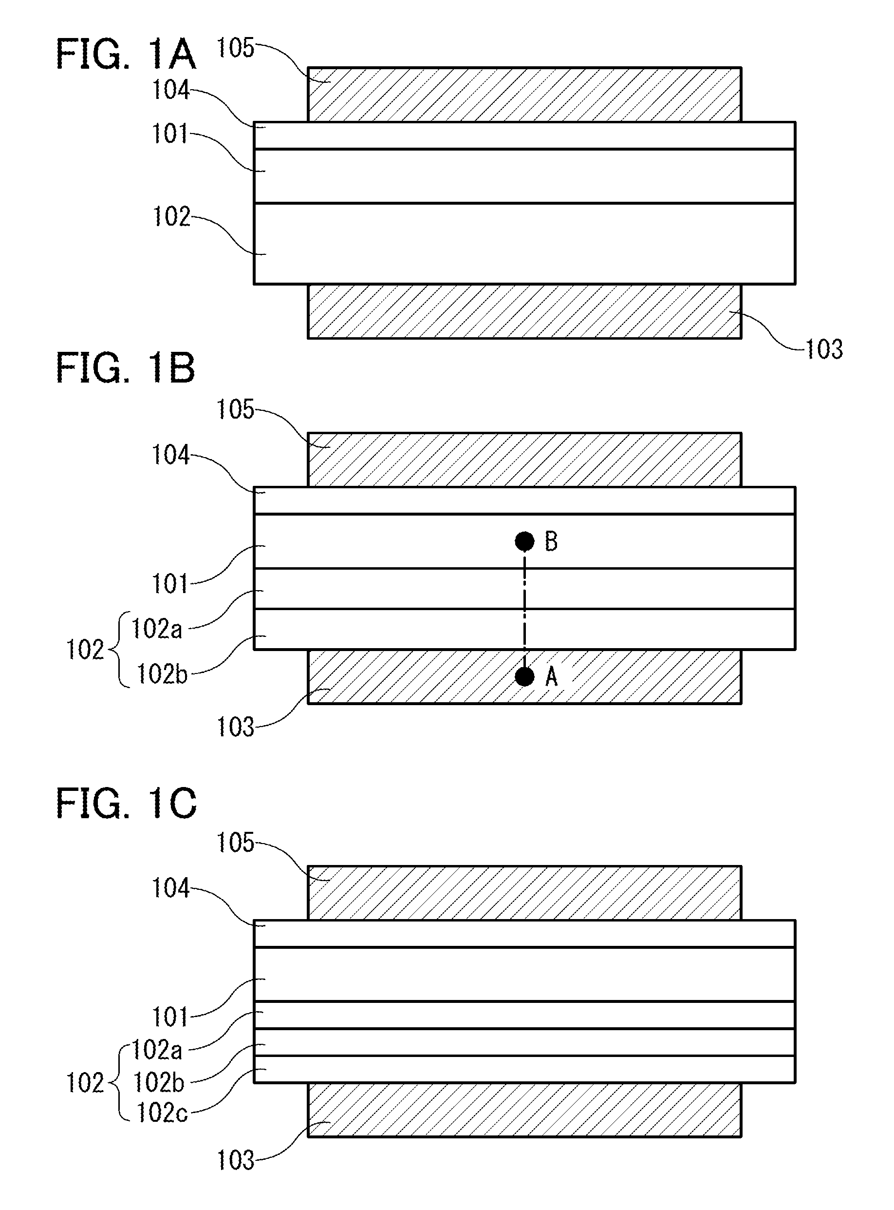
[0081]In this embodiment, a structure of a semiconductor device including a semiconductor, an electron trap layer, and a gate electrode, the operation principle of the semiconductor device, and a circuit that uses the semiconductor device are described. FIG. 1A shows a semiconductor device including a semiconductor 101, an electron trap layer 102, a gate electrode 103, a gate insulating layer 104, and a gate electrode 105.

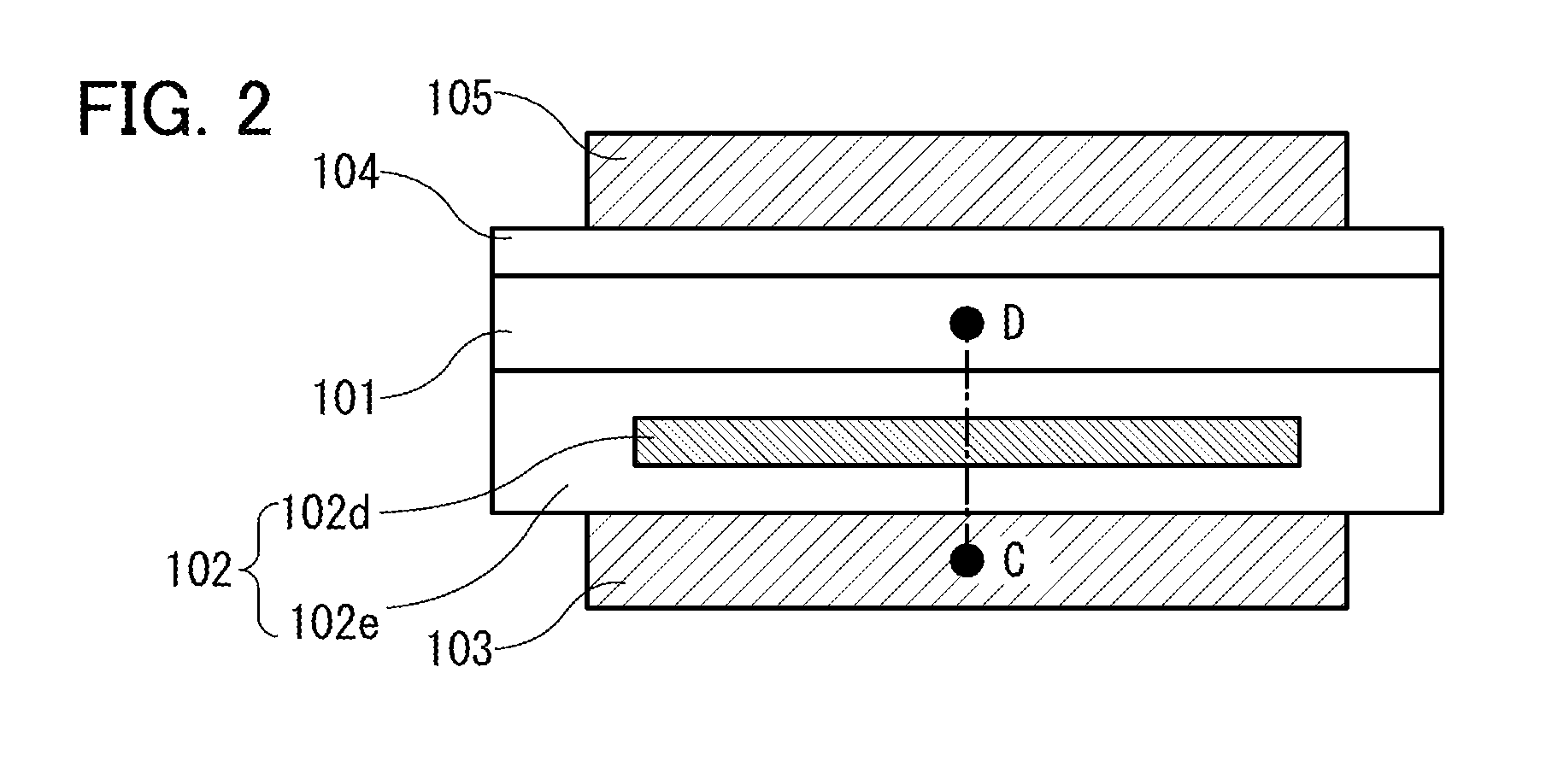
[0082]The electron trap layer 102 may be, for example, a stack including an insulator 102a and an insulator 102b as illustrated in FIG. 1B. Alternatively, the electron trap layer 102 may be a stack including the insulator 102a, the insulator 102b, and an insulator 102c as illustrated in FIG. 1C. Alternatively, the electron trap layer 102 may be a stack including more insulators. Alternatively, as illustrated in FIG. 2, the electron trap layer 102 may include an insulator 102e and an electrically isolated conductor 102d in the insulator 102e. The insulator 102e may ...

embodiment 2

[0121]In this embodiment, a structure of a transistor of one embodiment of the present invention is described with reference to drawings.

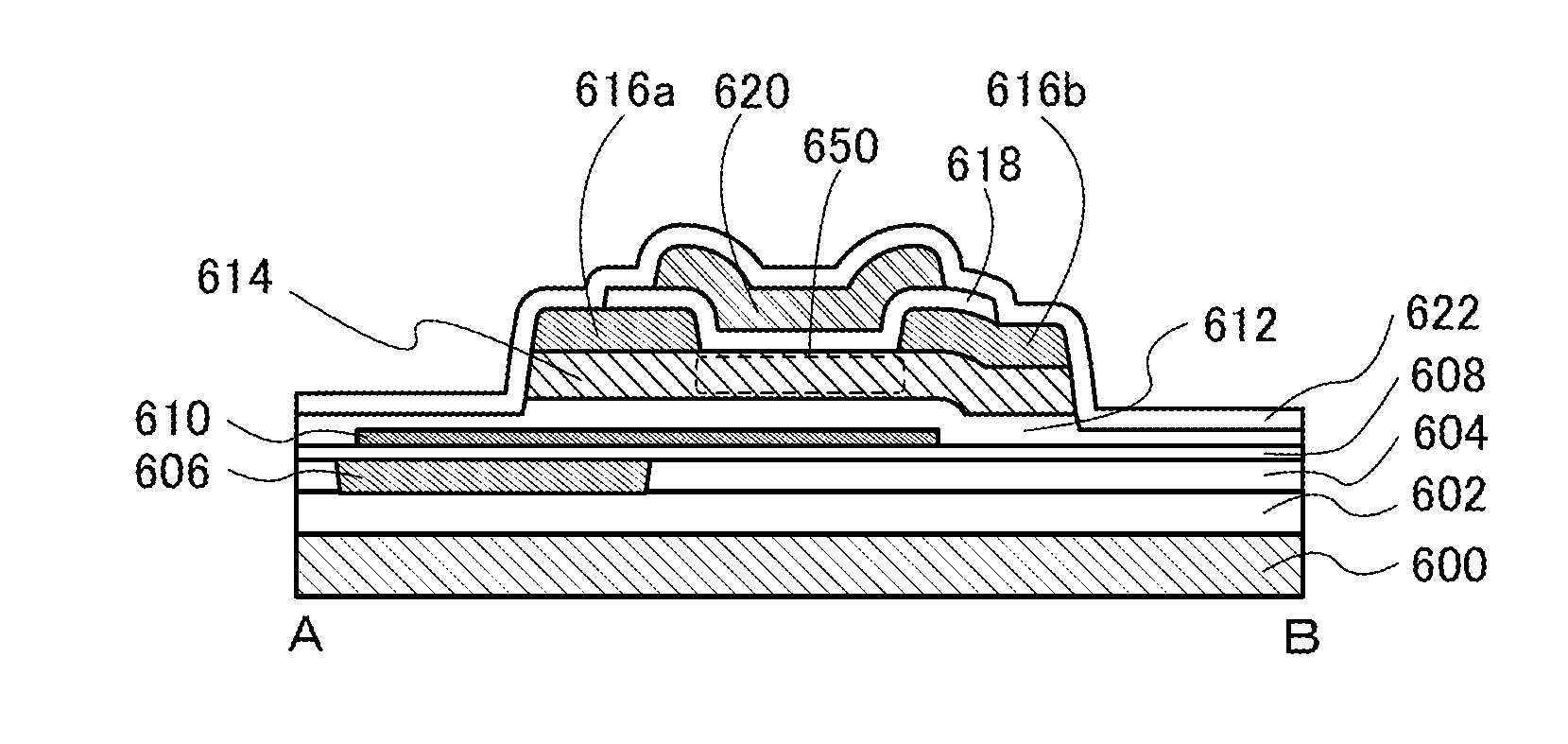
[0122]FIGS. 5A to 5C are a top view and cross-sectional views that illustrate a transistor of one embodiment of the present invention. FIG. 5A is the top view. FIG. 5B illustrates a cross section taken along the dashed-dotted line A-B in FIG. 5A. FIG. 5C illustrates a cross section taken along the dashed-dotted line C-D in FIG. 5A. Note that for simplification of the drawing, some components are not illustrated in the top view of FIG. 5A. In some cases, the direction of the dashed-dotted line A-B is referred to as a channel length direction, and the direction of the dashed-dotted line C-D is referred to as a channel width direction.

[0123]The transistor illustrated in FIGS. 5A to 5C includes an insulator 602 over a substrate 600; an insulator 604 over the insulator 602; a gate electrode 606 embedded in the insulator 604; an insulator 608 over the in...

embodiment 3

[0174]This embodiment describes a method for forming the transistor in FIGS. 5A to 5C, which is described in Embodiment 2, with reference to FIGS. 14A to 14C and FIGS. 15A to 15C.

[0175]A cross section taken along the dashed-dotted line A-B in FIG. 5A is illustrated in the left side of each of FIGS. 14A to 14C and FIGS. 15A to 15C. A cross section taken along the dashed-dotted line C-D in FIG. 5A is illustrated in the right side of each of FIGS. 14A to 14C and FIGS. 15A to 15C.

[0176]The insulator 602 is formed over the substrate 600. As the substrate 600, a single material semiconductor substrate of silicon, germanium, or the like or a compound semiconductor substrate of silicon carbide, silicon germanium, gallium arsenide, indium phosphide, zinc oxide, gallium oxide, or the like can be used, for example. Alternatively, an insulator substrate made of quartz, glass, or the like may be used. For the insulator 602, a silicon oxide film, a silicon oxynitride film, a silicon nitride oxide...


PUM


Abstract

A semiconductor device includes a first conductor, a second conductor, a first insulator, a second insulator, a third insulator, a semiconductor, and an electron trap layer. The semiconductor includes a channel formation region. The electron trap layer overlaps with the channel formation region with the second insulator interposed therebetween. The first conductor overlaps with the channel formation region with the first insulator interposed therebetween. The second conductor overlaps with the electron trap layer with the third insulator interposed therebetween. The second conductor does not overlap with the channel formation region.

Description

BACKGROUND OF THE INVENTION[0001]1. Field of the Invention[0002]The present invention relates to an object, a method, or a manufacturing method. The present invention relates to a process, a machine, manufacture, or a composition of matter. One embodiment of the present invention relates to a semiconductor device, a display device, a light-emitting device, a power storage device, an imaging device, a memory device, a driving method thereof, or a manufacturing method thereof. In particular, one embodiment of the present invention relates to a semiconductor device, a display device, or a light-emitting device each including an oxide semiconductor.[0003]In this specification and the like, a semiconductor device generally means a device that can function by utilizing semiconductor characteristics. A display device, a light-emitting device, a lighting device, an electro-optical device, a semiconductor circuit, and an electronic device include a semiconductor device in some cases.[0004]2....

Claims


Application Information

Patent Timeline
IPC IPC(8): H01L29/786H01L29/788
CPCH01L29/788H01L29/7869H01L27/1225H01L29/7881H01L27/14612H01L29/78606H01L27/1207H01L29/78696H01L29/78648H01L27/1255H10B41/70H10K59/1213H10K59/131H01L29/1083
Inventor TANAKA, TETSUHIROMATSUBAYASHI, DAISUKETANEMURA, KAZUKI
Owner SEMICON ENERGY LAB CO LTD
Why Eureka
Try Eureka