Vector processing architectures for infrared camera electronics

a technology of infrared camera and processing architecture, applied in the field of infrared camera electronic architecture, can solve the problems of unfavorable infrared imaging system size, power requirements, unfavorable cost, size and/or power requirements, and require significant processing speed of pixels, so as to efficiently exploit pixel-level parallelism, improve electronics architecture, and improve the effect of processing captured infrared image data

Active Publication Date: 2016-06-02
TELEDYNE FLIR LLC
View PDF2 Cites 13 Cited by
  • Summary
  • Abstract
  • Description
  • Claims
  • Application Information

AI Technical Summary

Benefits of technology

[0008]Systems and methods are disclosed herein for various embodiments to provide infrared imaging systems with improved electronics architectures. In one embodiment, an infrared imaging system is provided that includes an infrared imaging sensor for capturing infrared image data and a main electronics block for efficiently processing the captured infrared image data. The main electronics block may include a plurality of vector processors each configured to operate on multiple pixels of the infrared image data in parallel to efficiently exploit pixel-level parallelism. Each vector processor may be communicatively coupled to a local memory that provides high bandwidth, low latency access to a portion of the infrared image data for the vector processor operates on. The main electronics block may also include a general-purpose processor configured to manage data flow to / from the local memories and other system functionalities. The main electronics block may be implemented as a system-on-a-chip (SoC), further including a peripheral interface block.

Problems solved by technology

Such pixel processing requires significant processing speed, especially for real-time applications such as infrared cameras where videos / images need to be captured without significant latency or other delays.
However, such demand for processing speed often leads to unfavorable cost, size, and / or power requirements for infrared imaging systems with conventional image processing electronics architectures.
However, because PLDs are programmed using logic languages and have poor logic density compared to dedicated circuits, they are not well suited for implementing complex pixel processing algorithms such as resolution enhancement or other high-level pixel processing algorithms, or high-level functions such as networking, compression, user interface, file system management, or other functions of infrared cameras.
While some conventional infrared camera electronics include a general-purpose processor (e.g., a digital signal processor (DSP)) to perform such high-level functions, DSPs or other types of general-purpose processor typically cannot efficiently provide the processing speed for types of pixel processing desired in modem infrared cameras.
That is, a typical general-purpose processor either cannot meet the processing speed requirement or meets the processing speed requirement only with undesirably large power consumption and heat generation (e.g., running at high frequency).
However, hardwired electronics are more costly to implement, and more importantly do not offer the programmability or configurability to update or configure pixel processing operations as desired.
These difficulties are exacerbated by a growing demand for infrared imaging system electronics to provide video analytics, video compression, image enhancements, and other image / video processing, as well as the need to handle other system functionalities such as user interface, networking, image storage, and peripheral interface functionalities.
While some conventional infrared camera electronics aim to meet the increasing demand for processing speed by combining a general-purpose processor, a PLD, a peripheral controller, and other components, such a combination often results in increased cost, size, weight, and power requirements.

Method used


Image

  • Vector processing architectures for infrared camera electronics
  • Vector processing architectures for infrared camera electronics
  • Vector processing architectures for infrared camera electronics

Examples


Embodiment Construction

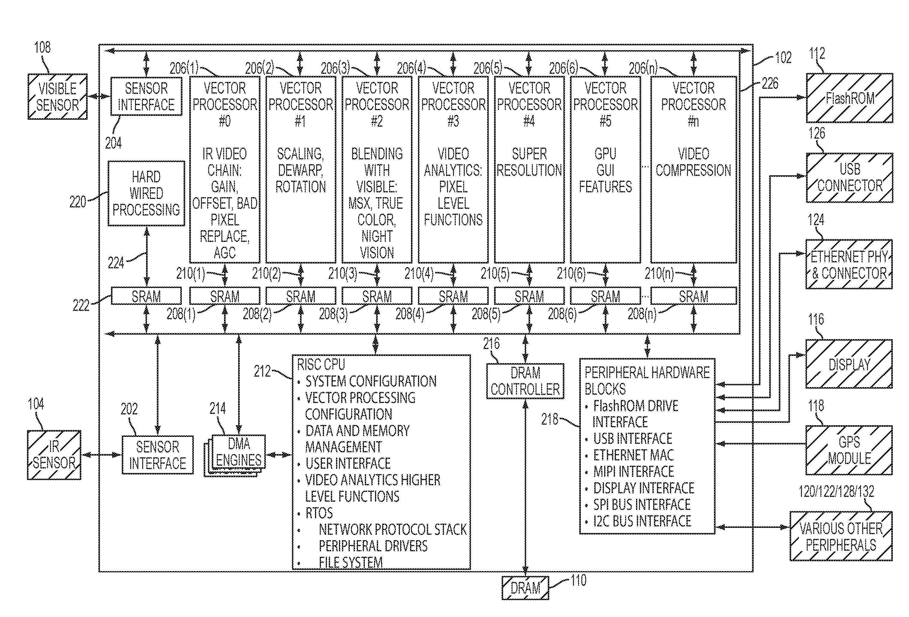
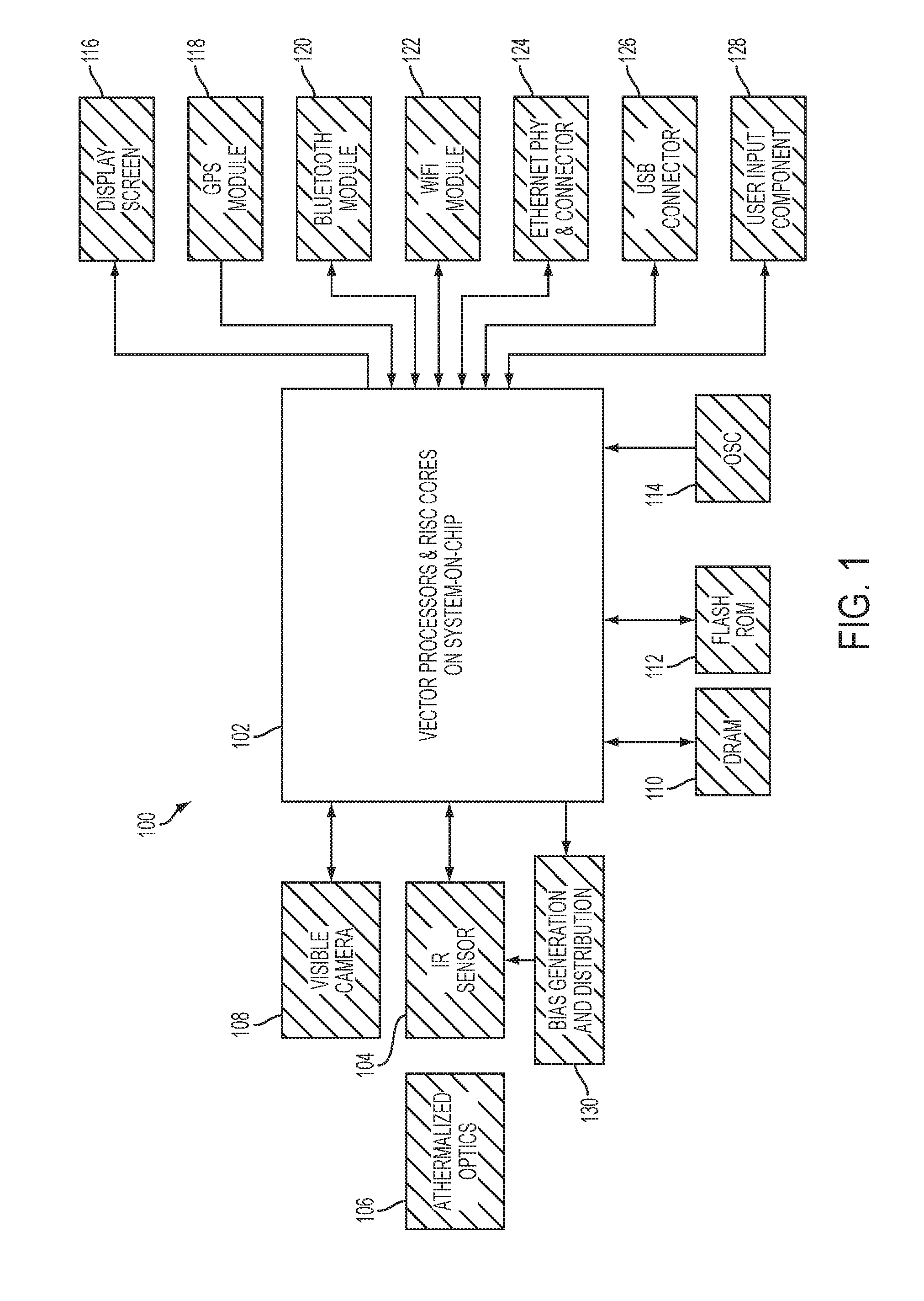
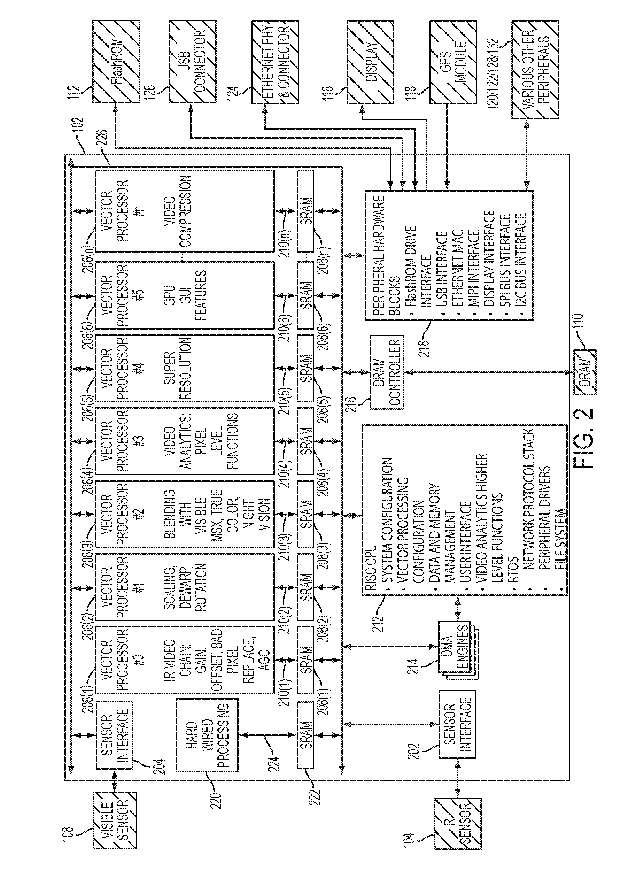
[0018]A video (or image) processing chain (e.g., one or more operations to process raw video / image data captured by an imaging sensor to produce a usable output video / image) for digital imaging devices such as infrared cameras may by nature have a high potential for data-level parallelism which is unexploited in conventional digital imaging devices. For example, many operations of a typical infrared camera video processing chain involve repetitions of a same independent pixel-level operation for every pixel in a video image frame. In addition to basic video processing chains, other more complex video processing and video analytics algorithms may also in part involve a pixel-level operation that is repeated independently for every pixel in a video image frame. Such repeating operations for multiple data elements (e.g., multiple pixels) can potentially be carried out in parallel.

[0019]Techniques are disclosed herein to provide efficient, scalable, flexible, yet cost-effective infrared...


PUM


Abstract

Systems and methods are disclosed herein to provide infrared imaging systems with improved electronics architectures. In one embodiment, an infrared imaging system is provided that includes an infrared imaging sensor for capturing infrared image data and a main electronics block for efficiently processing the captured infrared image data. The main electronics block may include a plurality of vector processors each configured to operate on multiple pixels of the infrared image data in parallel to efficiently exploit pixel-level parallelism. Each vector processor may be communicatively coupled to a local memory that provides high bandwidth, low latency access to a portion of the infrared image data for the vector processor to operate on. The main electronics block may also include a general-purpose processor configured to manage data flow to/from the local memories and other system functionalities. The main electronics block may be implemented as a system-on-a-chip.

Description

CROSS-REFERENCE TO RELATED APPLICATION[0001]This application is a continuation of International Application No. PCT / US2014 / 049828 filed Aug. 5, 2014 and entitled “VECTOR PROCESSING ARCHITECTURES FOR INFRARED CAMERA ELECTRONICS”, which is hereby incorporated by reference in its entirety.[0002]International Application No. PCT / US2014 / 049828 claims priority to and the benefit of U.S. Provisional Patent Application No. 61 / 862,923 filed Aug. 6, 2013 and entitled “VECTOR PROCESSING ARCHITECTURES FOR INFRARED CAMERA ELECTRONICS,” which is hereby incorporated by reference in its entirety.TECHNICAL FIELD[0003]One or more embodiments of the invention relate generally to electronics for imaging devices and more particularly, for example, to electronics architectures for infrared cameras.BACKGROUND[0004]Infrared imaging systems, such as infrared cameras, are increasing in popularity. As the cost to produce infrared imaging sensors decreases and the image quality improves, infrared imaging devic...

Claims


Application Information

Patent Timeline
Patent Type & Authority Applications(United States)
IPC IPC(8): H04N5/33H04N5/76
CPCH04N5/76H04N5/33G06T1/20
Inventor BOULANGER, PIERREROBERTS, RANDY
Owner TELEDYNE FLIR LLC
Why Eureka
Try Eureka