

High Gain Load Circuit for a Differential Pair Using Depletion Mode Transistors
a depletion-mode transistor and high-gain load technology, applied in the field of depletion-mode transistors, can solve the problems of limited gan transistor device choices, and inability to manufacture p-type gan devices, and achieve the effect of enhancing the gain stage of the differential pair and increasing the output impedan
- Summary
- Abstract
- Description
- Claims
- Application Information
AI Technical Summary
Benefits of technology
Problems solved by technology
Method used
Image

Examples
Embodiment Construction
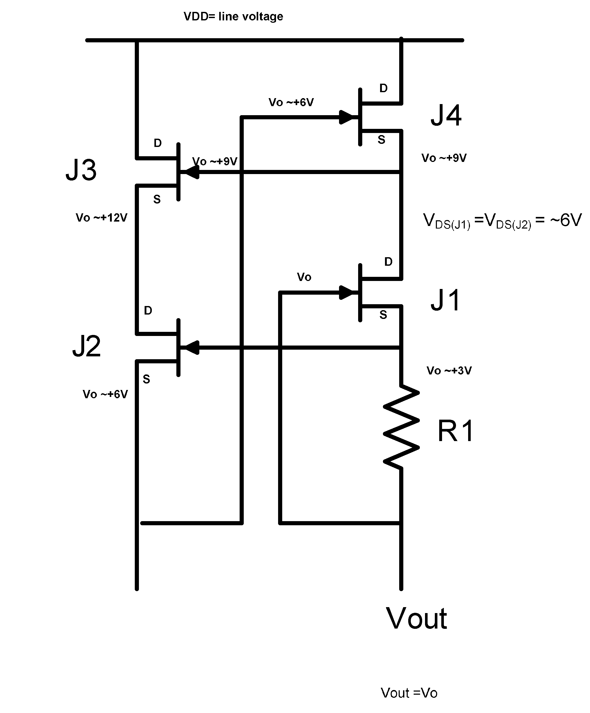
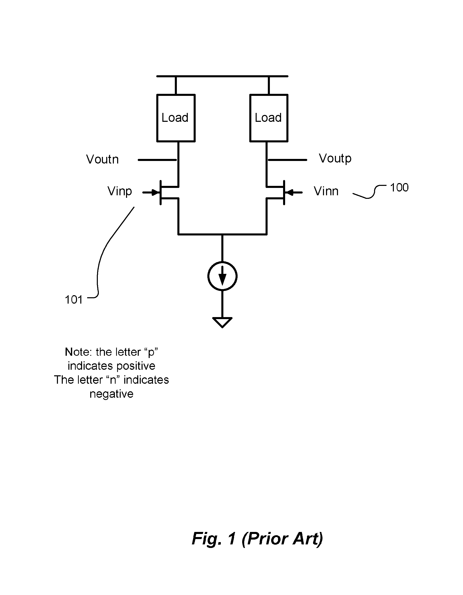
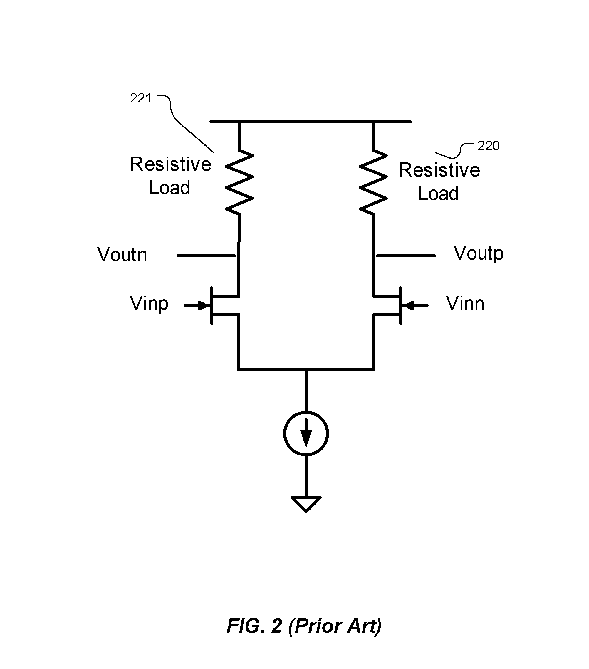
[0010]Embodiments of the invention include a depletion mode differential pair gain stage. The gain stage includes a differential pair of depletion-mode transistors, including a first and a second n-type transistor. In certain embodiments of the invention, the depletion mode transistor may be GaN (gallium nitride) field effect transistors. The transistors have a gate, source, and a drain and the differential pair coupled at the source of each transistor forming a common node. The gain stage also includes an active load including one or more depletion mode transistors electrically coupled to at least one of the drains of depletion mode transistors of the differential pair.
[0011]The differential pair may also include a constant current source coupled to a common node of the differential pair. The current source can be used for biasing the differential pair.
[0012]In embodiments of the invention, the active load includes a current source formed from a third depletion mode transistor coup...
PUM
 Abstract
Description
Claims
Application Information