Wafer level package for a MEMS sensor device and corresponding manufacturing process

a sensor device and manufacturing process technology, applied in the field of wafer level packages for microelectromechanical (mems) sensor devices and to a corresponding manufacturing process, can solve the problems of reducing the size of the package, affecting the performance of the sensor device, and not being compatible with many applications, etc., to achieve the effect of reducing the size and achieving the desired mechanical and electrical performan

Active Publication Date: 2016-06-30
STMICROELECTRONICS MALTA
View PDF4 Cites 5 Cited by
  • Summary
  • Abstract
  • Description
  • Claims
  • Application Information

AI Technical Summary

Benefits of technology

[0024]However, an altogether satisfactory packaging solution for a MEMS sensor device, having reduced size (e.g., in the vertical direction) and desired mechanical and electrical performances continues to be desired.

Problems solved by technology

This standard package assembly, although advantageous in many respects, suffers from some drawbacks.
In particular, the package 2 has a dimension (especially in the vertical direction z) that may not be compatible with many applications, where size is an important design parameter, e.g., in portable or wearable electronic devices.
Moreover, the electrical wires 6, 12 may be subject to breaking during the molding process, this leading to failure of the manufactured MEMS sensor device 1.
In particular, important issues that remain outstanding are how to provide electrical connections to the outside of the package, e.g., for soldering to an external printed circuit board, without resorting to the use of complex and expensive manufacturing process steps.

Method used


Image

  • Wafer level package for a MEMS sensor device and corresponding manufacturing process
  • Wafer level package for a MEMS sensor device and corresponding manufacturing process
  • Wafer level package for a MEMS sensor device and corresponding manufacturing process

Examples


Embodiment Construction

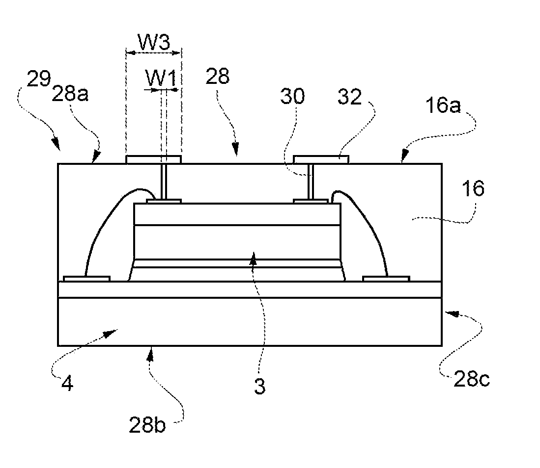
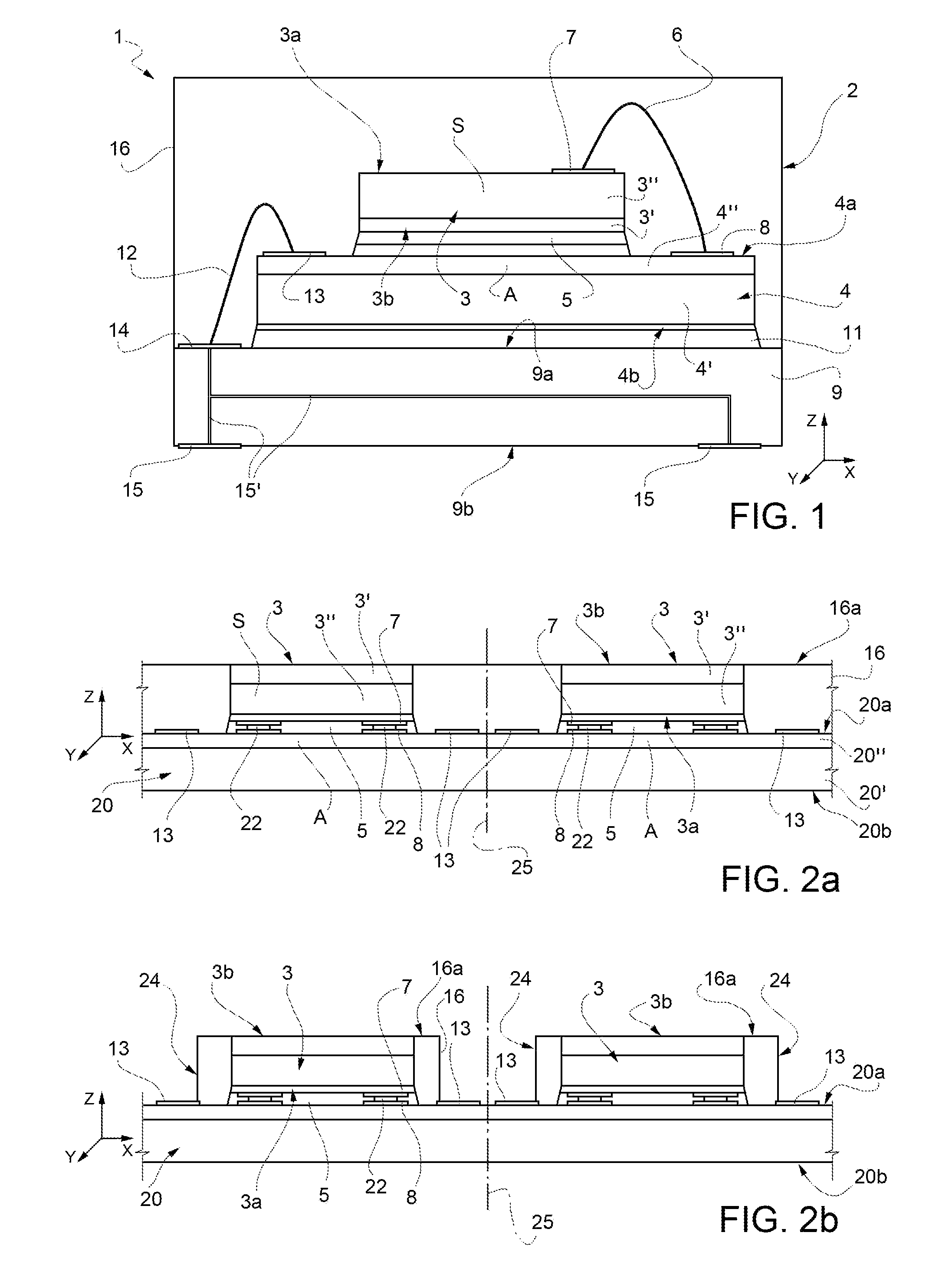
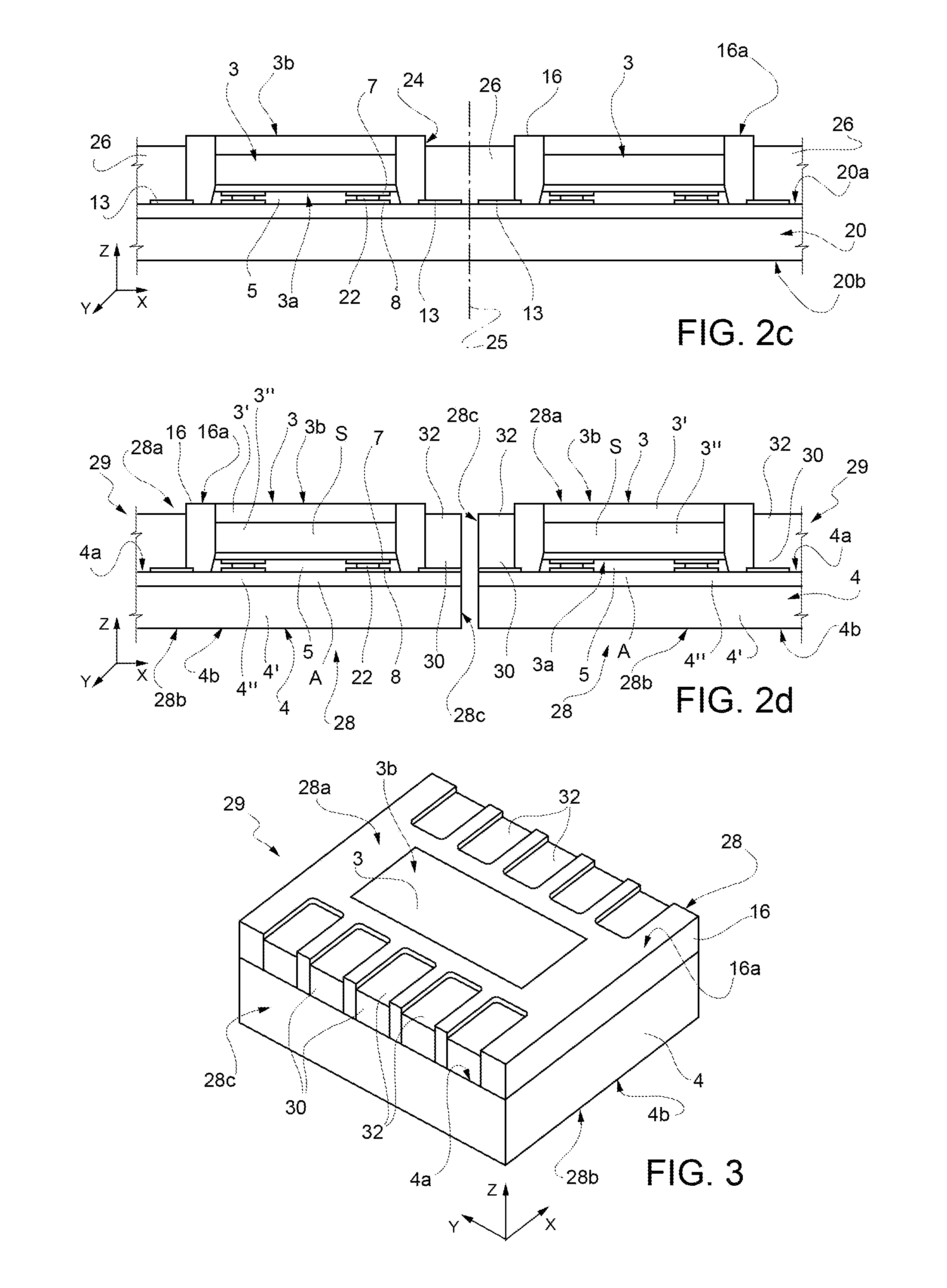
[0043]As will be detailed in the following discussion, an aspect of the present solution envisages a wafer-level packaging of a first die and a second die of semiconductor material, without any substrate as the base of the package; in possible embodiments, the first and second dies are preferably coupled with a flip-chip connection, without bonding with electrical wires.

[0044]In particular, vertical connection structures are envisaged through the thickness of a mold compound, coating at least in part the stack of first and second dies, reaching up to the external surface of the mold compound.

[0045]Moreover, in order to provide electrical connections to the outside of the package, e.g., for soldering to an external printed circuit board, external electrical connection elements, e.g., in the form of lands, are envisaged at the external surface of the mold compound, connected to the vertical connection structures.

[0046]According to a particular aspect of the present solution, the exter...


PUM

PropertyMeasurementUnit
adhesiveaaaaaaaaaa
adhesive solderableaaaaaaaaaa
conductiveaaaaaaaaaa

Abstract

A MEMS device having a wafer-level package, is provided with: a stack of a first die and a second die, defining at least a first internal surface internal to the package and carrying at least an electrical contact pad, and at least a first external surface external to the package and defining a first outer face of the package; and a mold compound, at least in part coating the stack of the first and second dies and having a front surface defining at least part of a second outer face of the package, opposite to the first outer face. The MEMS device is further provided with: at least a vertical connection structure extending from the contact pad at the first internal surface towards the front surface of the mold compound; and at least an external connection element, electrically coupled to the vertical connection structure and exposed to the outside of the package, at the second outer face thereof.

Description

BACKGROUND[0001]1. Technical Field[0002]The present disclosure relates to a wafer level package for a microelectromechanical (MEMS) sensor device and to a corresponding manufacturing process.[0003]2. Description of the Related Art[0004]As it is known, current packages for MEMS sensor devices, such as accelerometers, gyroscopes, magnetometers, pressure or force sensors, follow a standard process flow of die-attach of dies to a substrate, wire bonding and encapsulation.[0005]FIG. 1 shows an exemplary MEMS sensor device 1, with an LGA (Land Grid Array) package 2.[0006]The MEMS sensor device 1 includes a first die 3, including semiconductor material, e.g., silicon, and including a structural layer 3′ and an active layer 3″, wherein a micromechanical sensing structure S is integrated and includes, for example, a membrane suspended over a cavity, an inertial mass, elastic elements and / or other micromechanical sensing parts.[0007]First die 3 has a front surface 3a, defined by the active la...

Claims


Application Information

Patent Timeline
Patent Type & Authority Applications(United States)
IPC IPC(8): B81B7/00B81C1/00
CPCB81C1/00301B81B7/007B81B2207/098B81C2203/0154H01L23/3121H01L24/97H01L2224/04105H01L2224/16145H01L2224/16225H01L2224/32145H01L2224/32225H01L2224/48145H01L2224/48227H01L2224/73204H01L2224/73227H01L2224/73265H01L2224/92124H01L2224/92164H01L2224/94H01L2224/97H01L2924/0002H01L2924/181H01L2924/18161H01L2924/00012H01L2924/00H01L2224/81H01L2224/83H01L2224/85
Inventor CACHIA, CONRADVELLA, DAVID OSCARAGIUS, DAMIANSPITERI, MARIA
Owner STMICROELECTRONICS MALTA
Why Eureka
Try Eureka