Method of manufacturing nanowire array using induced growth
Inactive Publication Date: 2016-06-30
POSTECH ACAD IND FOUND
View PDF1 Cites 2 Cited by
Summary
Abstract
Description
Claims
Application Information
AI Technical Summary
This helps you quickly interpret patents by identifying the three key elements:
Problems solved by technology
Method used
Benefits of technology
Benefits of technology
This patent describes a way to make inorganic nanowires that are arranged horizontally and have precise position and structure. The method uses organic nanowires as a template to help induce the growth of the inorganic ones. This allows for easier patterning and shaping, making it easier to create complex structures using inorganic nanowires.
Problems solved by technology
However, inorganic semiconductor nanowires (Group IV semiconductors and compound semiconductors), which have been typically reported, are typically grown in a vertically aligned structure, and accurate length and diameter control may not only be difficult, but it may also be impossible to accurately adjust the number of nanowires.
In particular, even if an array having a vertically aligned structure is grown, it is highly difficult, in terms of processing, to apply the individual nanowire or nanowire array to an optical device or electronic device.
However, the method has limitations in that the patterning method may be difficult to provide a large-area pattern, may be expensive, and may only provide the array having a vertically aligned shape.
Although it is a very successful method in terms of the fact that gallium nitride nanowires may be grown on a sapphire substrate in a desired crystal direction, it is difficult to accurately control the number of nanowires as well as the diameter and length of the individual nanowire.
In addition, the method may have a limitation in that crystallographically restricted planes may only be used in the growth.
Image
Click on the blue label to locate the original text in one second.
Reading with bidirectional positioning of images and text.
Examples
example 1
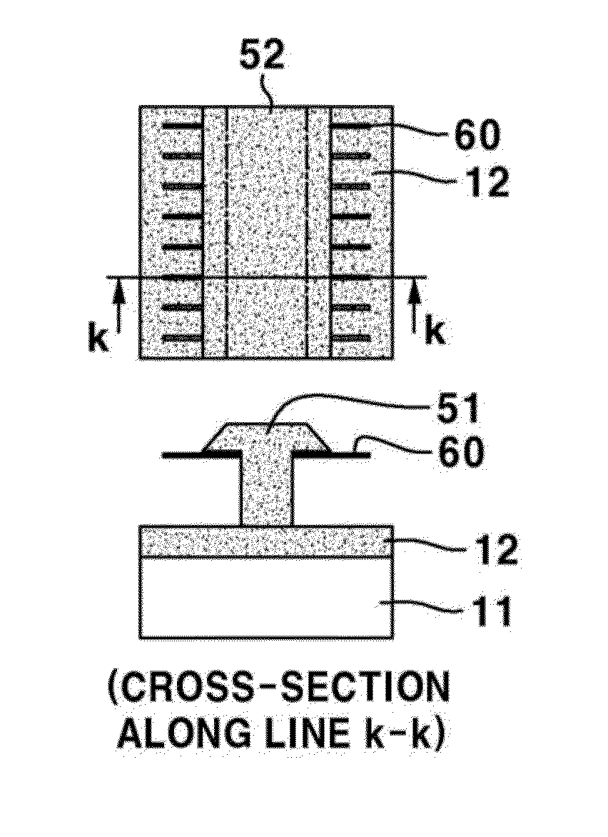
[0101]First, as in the example of FIGS. 1a-1k, an embodiment of step seed growth, in which a first seed layer 12 was formed on a substrate 11 of a base layer 10 and a second seed layer 51 was then formed stepwise so as to optimally form a second nanowire 60 finally formed in a nanotunnel 40, as an intermediate step, will be examined.
[0102]Basic embodiment steps and materials constituting configurations for each step or layer configuration follow basic descriptions of the method of manufacturing a nanowire array of the invention which have been previously described.
[0103]In addition to the basic descriptions, detailed configuration and steps of the embodiment of the step seed growth, as the first embodiment, will be examined.
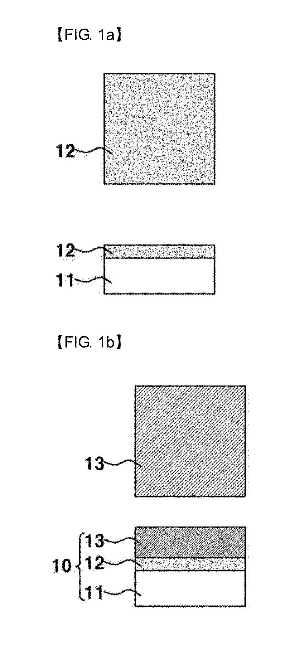
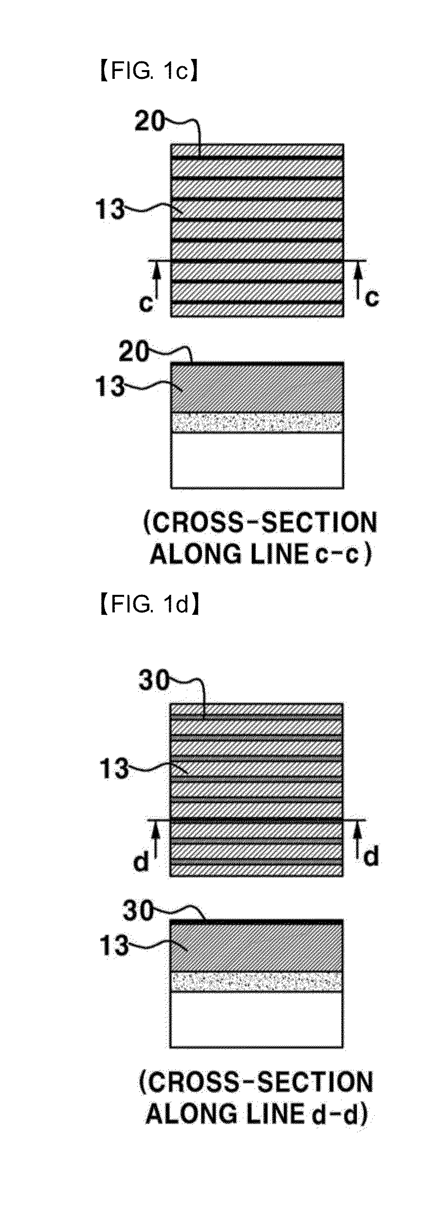
[0104]First, when a step of forming the base layer 10 and a first nanowire 20 is examined, a first seed layer forming step S110 of forming the first seed layer 12 on the substrate 11 was performed in the first embodiment.
[0105]That is, the first seed layer 12, as...
example 2
[0140]Next, as in the example of FIGS. 2a-2k, an embodiment of the batch seed growth, in which a seed tunnel was first formed on a substrate 11 of a base layer 10 and a second seed layer and a second nanowire 60 were formed together with respect to the seed tunnel and a nanotunnel 40 by using a first seed layer formed on the substrate 11 as a seed, will be examined.
[0141]With respect to the embodiment of the batch seed growth, as in the first embodiment, basic embodiment steps and materials constituting configurations for each step or layer configuration follow basic descriptions of the method of manufacturing a nanowire array of the invention which have been previously described.
[0142]In addition to the basic descriptions, detailed configuration and steps of the embodiment of the batch seed growth, as the second embodiment, will be examined.
[0143]First, as in the first embodiment, a first seed layer forming step S110 of forming a first seed layer 12 on the substrate 11 was performe...
PUM
Property
Measurement
Unit
Temperature
aaaaa
aaaaa
Temperature
aaaaa
aaaaa
Fraction
aaaaa
aaaaa
Abstract
Provided is a method of manufacturing a nanowire array using induced growth, in which a nitride inorganic nanowire is grown from a nitride seed by forming the nitride seed on a sapphire or silicon substrate, forming an organic nanowire pattern and a dielectric nanotunnel using the nanowire pattern as a template on the nitride seed, and using the nanotunnel as an induced growth mask.
Description
BACKGROUND OF THE INVENTION[0001]1. Field of the Invention[0002]The present invention relates to a method of growing a nanowire array, and more particularly, to a method of manufacturing a nanowire array using induced growth, in which nanotunnels are formed by using an organic nanowire array as a template and an aligned inorganic nanowire array is then formed by induced growth through the nanotunnels.[0003]2. Description of the Related Art[0004]Semiconductor nanowires, as an advanced device that may exceed the limitations of conventional semiconductor technology, have been recognized as an innovative key technology in various semiconductorapplication areas and have been particularly in the spotlight in electronic and optical device applications. In the electronic device applications, a significant amount of research related to transistors and memory devices using nanowires has been conducted. Research into solar cells and light-emitting devices in the optical device applications an...
Claims
Application Information
Patent Timeline
Application Date:The date an application was filed.
Publication Date:The date a patent or application was officially published.
First Publication Date:The earliest publication date of a patent with the same application number.
Issue Date:Publication date of the patent grant document.
PCT Entry Date:The Entry date of PCT National Phase.
Estimated Expiry Date:The statutory expiry date of a patent right according to the Patent Law, and it is the longest term of protection that the patent right can achieve without the termination of the patent right due to other reasons(Term extension factor has been taken into account ).
Invalid Date:Actual expiry date is based on effective date or publication date of legal transaction data of invalid patent.

