Solid-state imaging device and electronic apparatus

a solid-state imaging and electronic equipment technology, applied in the direction of electrical equipment, semiconductor devices, radio frequency controlled devices, etc., can solve the problem of low shape precision and achieve the effect of low shape precision

Active Publication Date: 2016-07-07
SONY CORP
View PDF7 Cites 3 Cited by
  • Summary
  • Abstract
  • Description
  • Claims
  • Application Information

AI Technical Summary

Benefits of technology

[0005]In solid-state imaging devices including white pixels, color mixture of the white pixels with adjacent colored pixels may occur easily. To restrain color mixture has been therefore desired. Moreover, when the clear layers are made of the same material as that of the interlayer insulating film as the underlayer, etching treatment of the clear layer becomes difficult, causing lower shape precision.
[0006]It is therefore desirable to provide a solid-state imaging, device that makes it possible to restrain color mixture and to improve shape precision, and an electronic apparatus including the solid-state imaging device.
[0008]In the solid-state imaging device according to the embodiment of the disclosure, the refractive index of the clear layer is higher than the refractive index of the colored filter. Thus, light obliquely entering the clear layer is reflected at an interface between the clear layer and the colored filter, and the reflected light is returned toward the clear layer. This leads to a decrease in an amount of light that passes through the clear layer to enter adjacent pixels, restraining color mixture of the white pixels with adjacent colored pixels. Moreover, the clear layer includes the inorganic dielectric film made of the different material from the material of the interlayer insulating film. This makes it possible to control an etching amount of the clear layer with high precision, leading to improvement in shape precision.
[0011]According to the solid-state imaging device according to the embodiment of the disclosure, or the electronic apparatus according to the embodiment of the disclosure, the refractive index of the clear layer is higher than the refractive index of the colored filter. Hence, it is possible to reduce the amount of light passing through the clear layer and entering adjacent pixels, and to restrain color mixture of the white pixels with the adjacent colored pixels. Moreover, the clear layer includes the inorganic dielectric film made of the different material from the material of the interlayer insulating film. Hence, it is possible to control the etching amount of the clear layer with high precision, leading to improvement in shape precision.

Problems solved by technology

Moreover, when the clear layers are made of the same material as that of the interlayer insulating film as the underlayer, etching treatment of the clear layer becomes difficult, causing lower shape precision.

Method used


Image

  • Solid-state imaging device and electronic apparatus
  • Solid-state imaging device and electronic apparatus
  • Solid-state imaging device and electronic apparatus

Examples


first embodiment

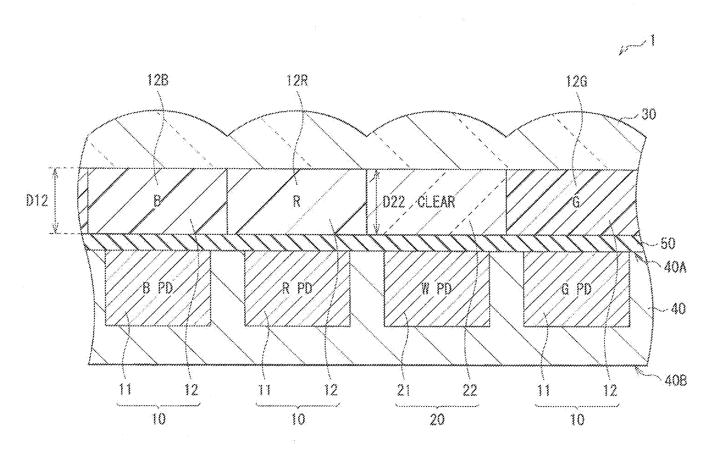
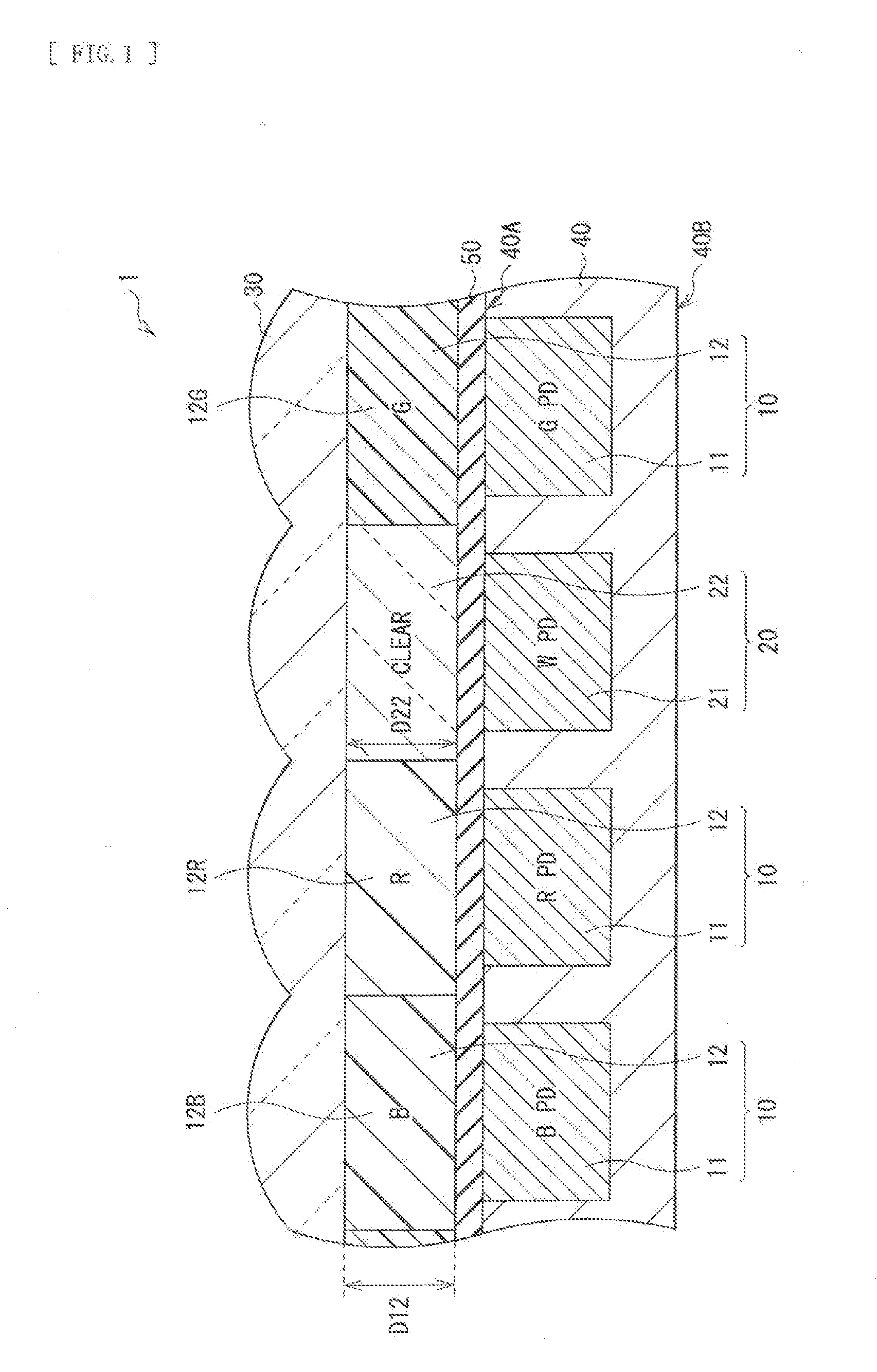
[0065]FIG. 1 illustrates a cross-sectional configuration of a solid-state imaging device according to a first embodiment of the disclosure. The solid-state imaging device 1 may be a CMOS image sensor used in electronic apparatuses such as digital still cameras and video cameras, and may include an imaging pixel region (a later-described pixel unit 110) in which a plurality of colored pixels 10 and a plurality of white pixels 20 are two-dimensionally arranged. The solid-state imaging device 1 may be either of a backside illuminated type or of a front illuminated type; here, for purpose of example, description is given of a structure of the backside illuminated type.

[0066]The colored pixels 10 each include, for example, a first photoelectric conversion element 11 and a colored filter 12. The colored pixels 10 each are adapted to detect a wavelength of either one of for example, red (R), green (G), and blue (B). The first photoelectric conversion element 11 may include a photodiode. Th...

second embodiment

[0099]Description is given next on a method of manufacturing the solid-state imaging device 1 according to a second embodiment of the disclosure. The method of manufacture relates to a case of manufacture of the solid-state imaging device 1 including the unit array U2 in which, as illustrated in FIG. 20, the green pixel 10G on the lower right in the RGB Bayer array is replaced with the white pixel 20.

[0100]FIGS. 21 to 28 illustrate the method of manufacturing the solid-state imaging device 1 according to the embodiment in the order of procedure. First, as illustrated in FIG. 21, the first photoelectric conversion element 11 and the second photoelectric conversion element 21 may be formed on the substrate 40 made of silicon (Si). Next, the transfer transistor, the FD, the multi-layered wirings, and other components (none of which is illustrated) may be formed on the front surface 40B of the substrate 40, on which the support substrate (not illustrated) may be bonded. Subsequently, th...

third embodiment

[0110]In the following, description is given on a method of manufacturing the solid-state imaging device 1 according to a third embodiment of the disclosure. The method of manufacture relates to a case of manufacture of the solid-state imaging device 1 including the unit array U1 in which, as illustrated in FIG. 31, the two green pixels 10G in the RGB Bayer array are replaced with the white pixels 20.

[0111]FIGS. 32 to 40 illustrate the method of manufacturing the solid-state imaging device 1 in the order of procedure. First, as illustrated in FIG. 32, the first photoelectric conversion element 11 and the second photoelectric conversion element 21 may be formed on the substrate 40 made of silicon (Si). Next, the transfer transistor, the FD, the multi-layered wirings, and other components (none of which is illustrated) may be formed on the front surface 40B of the substrate 40, on which the support substrate (not illustrated) may be bonded. Subsequently, the substrate 40 may be revers...


PUM


Abstract

There is provided a solid-state imaging device that includes: colored pixels each including a first photoelectric conversion element and a colored filler; white pixels each including a second photoelectric conversion element and a clear layer; and an interlayer insulating film provided between the first photoelectric conversion element and the colored filter, and between the second photoelectric conversion element and the clear layer. The colored filter is provided on light-entering side of the first photoelectric conversion element. The clear layer is provided on light-entering side of the second photoelectric conversion element. The clear layer has a higher refractive index than a refractive index of the colored filter, and includes an inorganic dielectric film made of a different material from a material of the interlayer insulating film.

Description

TECHNICAL FIELD[0001]The disclosure relates to a solid-state imaging device including white pixels, and an electronic apparatus including the solid-state imaging device.BACKGROUND ART[0002]CMOS (Complementary Metal-Oxide Semiconductor) image sensors may exemplify solid-state imaging devices installed in digital video cameras, digital still cameras, tablet computers, smartphones, mobile phones, etc. In CMOS image sensors, photoelectric charges are accumulated in pn junction capacitance of photodiodes (PDs) that serve as photoelectric conversion elements; the photoelectric charges thus accumulated are read out through MOS transistors.[0003]In solid-state imaging devices, micro-miniaturization of pixel sizes is being promoted in accordance with an increase in the number of pixels. Micro-miniaturization is accompanied by a shrink of PD area and a decrease in an amount of entering light, causing lower sensitivity. To compensate the lower sensitivity, white pixels have come into use inste...

Claims


Application Information

Patent Timeline
Patent Type & Authority Applications(United States)
IPC IPC(8): H01L27/146
CPCH01L27/14623H01L27/14645H01L27/1462H01L27/14621H01L27/14625H01L27/1464H01L27/14685
Inventor NATORI, TAICHI
Owner SONY CORP
Why Eureka
Try Eureka