Method of manufacturing semiconductor device, substrate processing apparatus, substrate processing system and recording medium

a semiconductor and processing apparatus technology, applied in the direction of coatings, chemical vapor deposition coatings, metallic material coating processes, etc., can solve the problems of inability to form thin films with sufficient etching resistance, difficult to add a sufficient amount of carbon to the films, and low dielectric constant, so as to improve the resistance to wet etching and improve the film quality. , the effect of reducing the dielectric constan

Active Publication Date: 2016-07-21
KOKUSA ELECTRIC CO LTD
View PDF6 Cites 322 Cited by
  • Summary
  • Abstract
  • Description
  • Claims
  • Application Information

AI Technical Summary

Benefits of technology

[0006]Also, when a thin film containing carbon and the like is formed on a substrate, it is possible to improve quality of the film, for example, improvement of resistance to wet etching, reduction of a dielectric constant of the film and the like.

Problems solved by technology

However, at a relatively low temperature, it is difficult for a sufficient amount of carbon to be added to the film or an impurity such as moisture is possible to be mixed into the film.
Therefore, there is a problem in that the thin film having sufficient etching resistance and a low dielectric constant may not be formed.

Method used


Image

  • Method of manufacturing semiconductor device, substrate processing apparatus, substrate processing system and recording medium
  • Method of manufacturing semiconductor device, substrate processing apparatus, substrate processing system and recording medium
  • Method of manufacturing semiconductor device, substrate processing apparatus, substrate processing system and recording medium

Examples


first embodiment

[0028]Hereinafter, a first embodiment of the present invention will be described with reference to the drawings.

[0029](1) Overall Configuration of Substrate Processing Apparatus

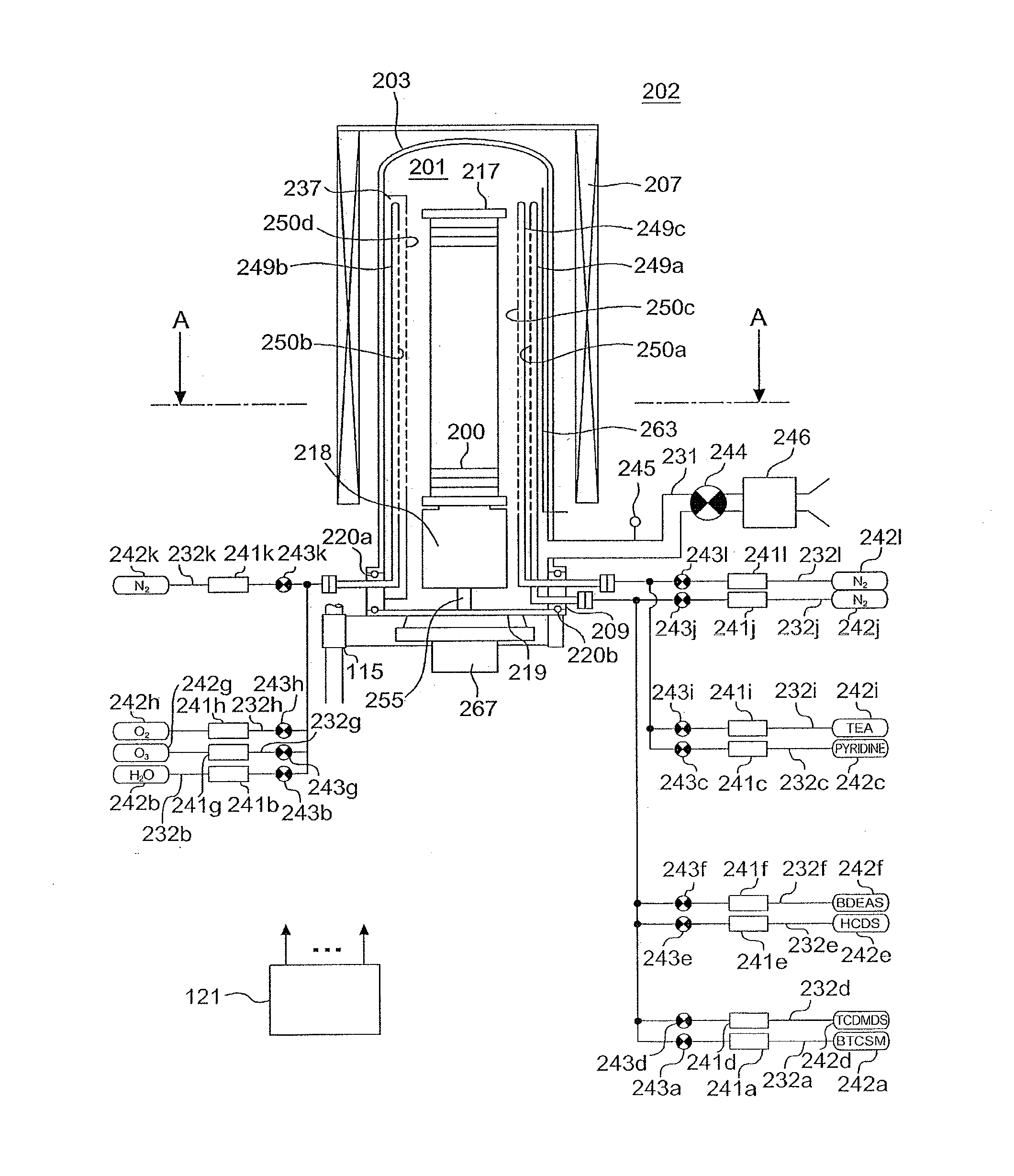
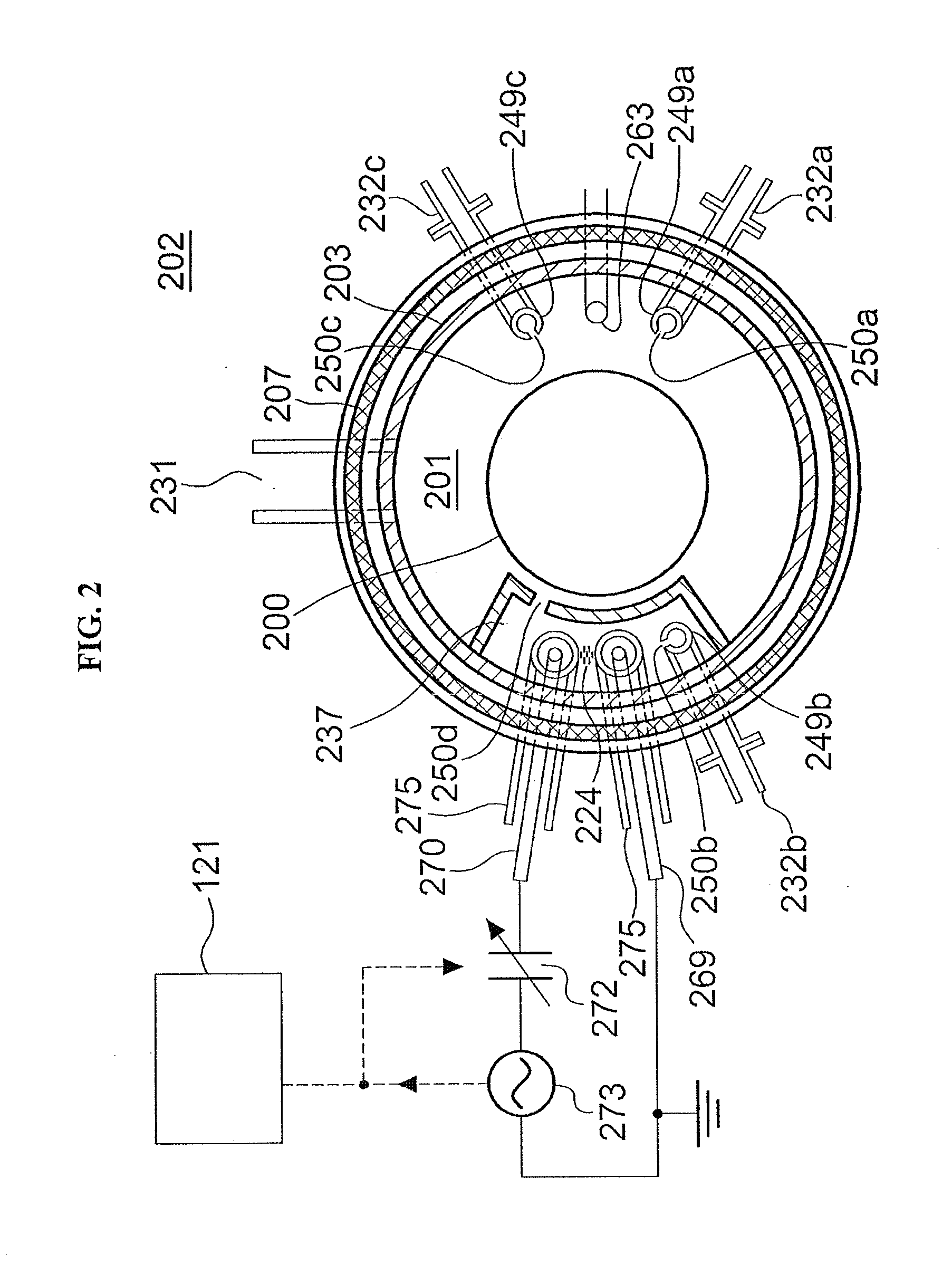
[0030]As illustrated in FIG. 1, a processing furnace 202 includes a heater 207 serving as a heating unit (a heating mechanism). The heater 207 has a cylindrical shape and is vertically installed by being supported by a heat base (not illustrated) serving as a holding plate. Also, the heater 207 also serves as an activating mechanism (an exciting unit) for activating (exciting) a gas by heat as will be described later.

[0031]In the heater 207, a reaction tube 203 is concentrically provided with respect to the heater 207. The reaction tube 203 is made of a heat-resistant material such as quartz (SiO2), carbide (SiC) or the like, and is formed to have a cylindrical shape whose upper end is closed and whose lower end is open. A manifold 209 (an inlet flange) is concentrically provided with respect to the reaction ...

third embodiment

[0294]Next, a third embodiment of the present invention will be described.

[0295](1) Stacked Film Forming Process

[0296]According to the above-described embodiment, the SiOC film is formed by performing a cycle including steps S1a and S2a or steps S1c and S2c a predetermined number of times. According to the present embodiment, with the above-described SiOC film forming process, a process of supplying a chlorosilane-based source gas different from the above-described gases while supplying a catalytic gas to the wafer 200 and a process of supplying an oxidizing gas while supplying the catalytic gas to the wafer 200 are performed the predetermined number of times. Thus, a stacked film of the SiOC film and an SiO film different from the SiOC film is formed.

[0297]Hereinafter, a film-forming sequence of the present embodiment will be described with reference to FIGS. 10 and 11. In the present embodiment, the substrate processing apparatus illustrated in FIGS. 1 and 2 is also used as in the...

embodiments

First Embodiment

[0387]According to the embodiment of the present invention, the SiOC film is formed on the wafer by the film-forming sequence according to the above-described embodiment illustrated in FIGS. 7A and 7B using the substrate processing apparatus of the above-described embodiment, and various characteristics of the SiOC film are evaluated by performing the modifying process on the SiOC film. As the modifying process of the SiOC film, the second thermal processing is performed only without performing the first thermal processing. In this case, BTCSM gas is used as a source gas, H2O gas is used as an oxidizing gas, a pyridine gas is used as a catalytic gas, and N2 gas is used as a thermal processing gas when performing the modifying process of the SiOC film. The process conditions are the same as the process conditions in the above-described embodiment.

[0388]FIGS. 16A through 16C are graphs illustrating evaluation results of the present embodiment, where FIG. 16A is a graph...


PUM


Abstract

There is provided a technique including: (a) forming a thin film containing a predetermined element, oxygen and carbon on a substrate by performing a cycle a predetermined number of times, the cycle including: (a-1) supplying a source gas containing the predetermined element, carbon and a halogen element having a chemical bond between the predetermined element and carbon to the substrate; (a-2) supplying an oxidizing gas to the substrate; and (a-3) supplying a catalytic gas to the substrate; (b) removing a first impurity from the thin film by thermally processing the thin film at a first temperature higher than a temperature of the substrate in (a); and (c) removing a second impurity different from the first impurity from the thin film by thermally processing the thin film at a second temperature equal to or higher than the first temperature after performing (b).

Description

CROSS-REFERENCE TO RELATED PATENT APPLICATION[0001]This non-provisional U.S. patent application claims priority under 35 U.S.C. §119 of PCT / JP2013 / 076571, filed on Sep. 30, 2013, the entire contents of which are hereby incorporated by reference.BACKGROUND OF THE INVENTION[0002]1. Field of the Invention[0003]The present invention relates to a method of manufacturing a semiconductor device, a substrate processing apparatus, a substrate processing system and a recording medium.[0004]2. Description of the Related Art[0005]As one of processes of manufacturing a semiconductor device, a thin film such as a silicon oxide film and the like may be formed on a substrate by supplying a source gas containing a predetermined element such as silicon and the like and an oxidizing gas to the substrate. For example, when the thin film is formed using a catalytic gas, it is possible to form a film at a relatively low temperature, and thus thermal history and the like acting on the semiconductor device...

Claims


Application Information

Patent Timeline
Patent Type & Authority Applications(United States)
IPC IPC(8): H01L21/02C23C16/455C23C16/52
CPCH01L21/0228H01L21/02126H01L21/02211C23C16/45544H01L21/02318C23C16/52H01L21/02208C23C16/30C23C16/401C23C16/45534C23C16/45536H01L21/02164H01L21/022
Inventor NODA, TAKAAKINOHARA, SHINGOSHIMAMOTO, SATOSHIASHIHARA, HIROSHIHANASHIMA, TAKEOHIROSE, YOSHIROKAMAKURA, TSUKASA
Owner KOKUSA ELECTRIC CO LTD
Why Eureka
Try Eureka