High efficiency leds and methods of manufacturing

Active Publication Date: 2016-07-21
CREELED INC
View PDF14 Cites 15 Cited by
  • Summary
  • Abstract
  • Description
  • Claims
  • Application Information

AI Technical Summary

Benefits of technology

[0011]The present invention relates to simplified chip architectures or chip builds that can result in simpler manufacturing processes using fewer steps

Problems solved by technology

For conventional LEDs with a single out-coupling surface, the external quantum efficiency can be limited by a number of factors, such as total internal reflection (TIR) of light from the LED's emission region.
While the reflective cup 13 may direct light in an upward direction, optical losses may occur when the light is

Method used


Image

  • High efficiency leds and methods of manufacturing
  • High efficiency leds and methods of manufacturing
  • High efficiency leds and methods of manufacturing

Examples


Example

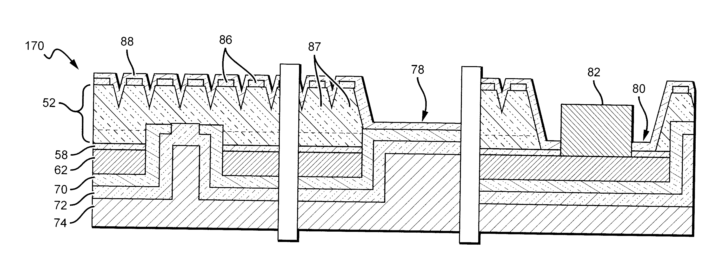
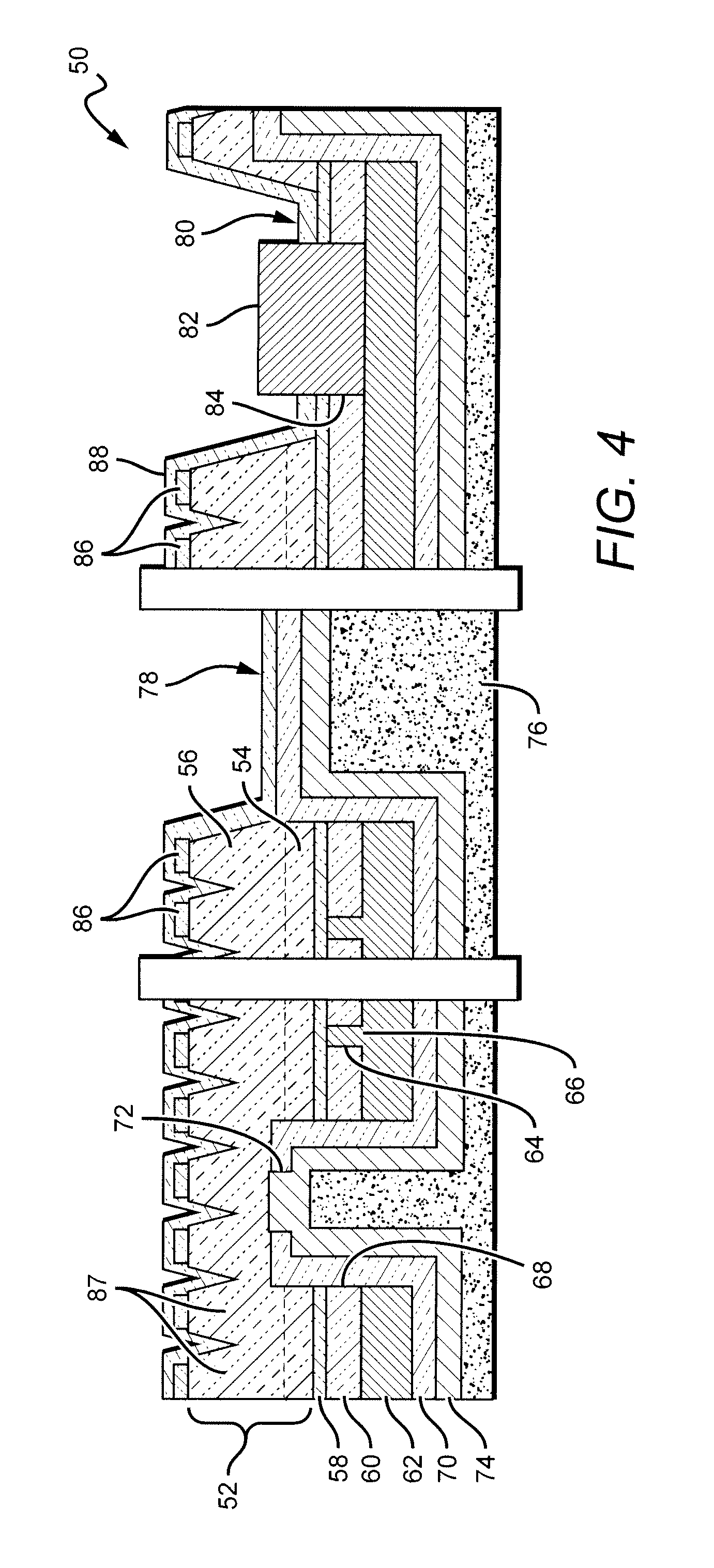
[0031]The present invention is directed to simplified LED chip structures / builds that can be fabricated using methods with fewer steps, while still providing LED chips with efficient light emission. The present invention is directed to LED chips having internal or integral reflective surfaces / layers arranged to increase the emission efficiency of the emitters. The present invention can be used as a reflector in conjunction with one or more contacts, or can be used as a reflector separate from the contacts.

[0032]The LED chips according to the present invention can comprise an active LED structure. A dielectric reflective layer is included adjacent to one of the oppositely doped layers. A metal reflective layer is on the dielectric reflective layer, wherein the dielectric and metal reflective layers extend beyond the edge of said active region. By extending the dielectric layer, the LED chips can emit with more efficiency by reflecting more LED light to emit in the desired direction. ...


PUM


Abstract

Simplified LED chip architectures or chip builds are disclosed that can result in simpler manufacturing processes using fewer steps. The LED structure can have fewer layers than conventional LED chips with the layers arranged in different ways for efficient fabrication and operation. The LED chips can comprise an active LED structure. A dielectric reflective layer is included adjacent to one of the oppositely doped layers. A metal reflective layer is on the dielectric reflective layer, wherein the dielectric and metal reflective layers extend beyond the edge of said active region. By extending the dielectric layer, the LED chips can emit with more efficiency by reflecting more LED light to emit in the desired direction. By extending the metal reflective layer beyond the edge of the active region, the metal reflective layer can serve as a current spreading layer and barrier, in addition to reflecting LED light to emit in the desired direction. The LED chips can also comprise self-aligned and self-limiting features that simplify etching processes during fabrication.

Description

BACKGROUND OF THE INVENTION[0001]1 Field of the Invention[0002]This invention relates to light emitting diodes, and more particularly to light emitting diodes having high reflectivity mirrors.[0003]2. Description of the Related Art[0004]Light emitting diodes (LED or LEDs) are solid state devices that convert electric energy to light, and generally comprise one or more active layers of semiconductor material sandwiched between oppositely doped n-type and p-type layers. When a bias is applied across the doped layers, holes and electrons are injected into the active layer where they recombine to generate light. Light is emitted from the active layer and from all surfaces of the LED.[0005]For typical LEDs it is desirable to operate at the highest light emission efficiency, and one way that emission efficiency can be measured is by the emission intensity in relation to the input power, or lumens per watt. One way to maximize emission efficiency is by maximizing extraction of light emitte...

Claims


Application Information

Patent Timeline
IPC IPC(8): H01L33/46H01L33/38H01L33/00H01L33/14
CPCH01L33/46H01L33/14H01L2933/0025H01L33/0095H01L2933/0016H01L33/38H01L33/42
Inventor DONOFRIO, MATTHEWKAR, PRITISHHEIKMAN, STENGOLAKIA, HARSHADACHARYA, RAJEEVDORA, YUVARAJ
Owner CREELED INC
Why Eureka
Try Eureka