Silicon carbide semiconductor device and method of manufacturing the same

a technology of silicon carbide and semiconductor devices, which is applied in the direction of semiconductor devices, electrical devices, transistors, etc., can solve the problems of difficult thermal diffusion process doping of impurities, extremely low coefficient of diffusion of impurities in silicon carbide, etc., and achieve high manufacturing efficiency

Active Publication Date: 2016-07-28
SUMITOMO ELECTRIC IND LTD
View PDF22 Cites 5 Cited by
  • Summary
  • Abstract
  • Description
  • Claims
  • Application Information

AI Technical Summary

Benefits of technology

[0009]According to the present invention, a silicon carbide semiconductor device which can be manufactured at high manufacturing efficiency and a method of manufacturing the same can be provided.

Problems solved by technology

Since silicon carbide is extremely low in coefficient of diffusion of an impurity, doping with an impurity through a thermal diffusion process is difficult.

Method used


Image

  • Silicon carbide semiconductor device and method of manufacturing the same
  • Silicon carbide semiconductor device and method of manufacturing the same
  • Silicon carbide semiconductor device and method of manufacturing the same

Examples


first embodiment

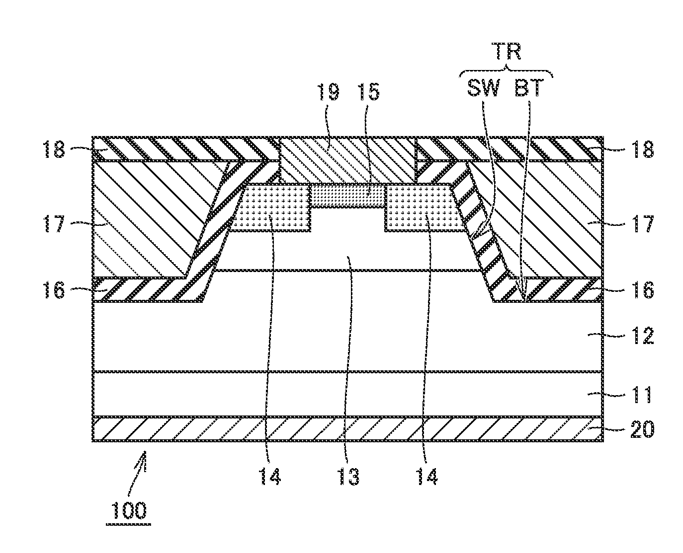
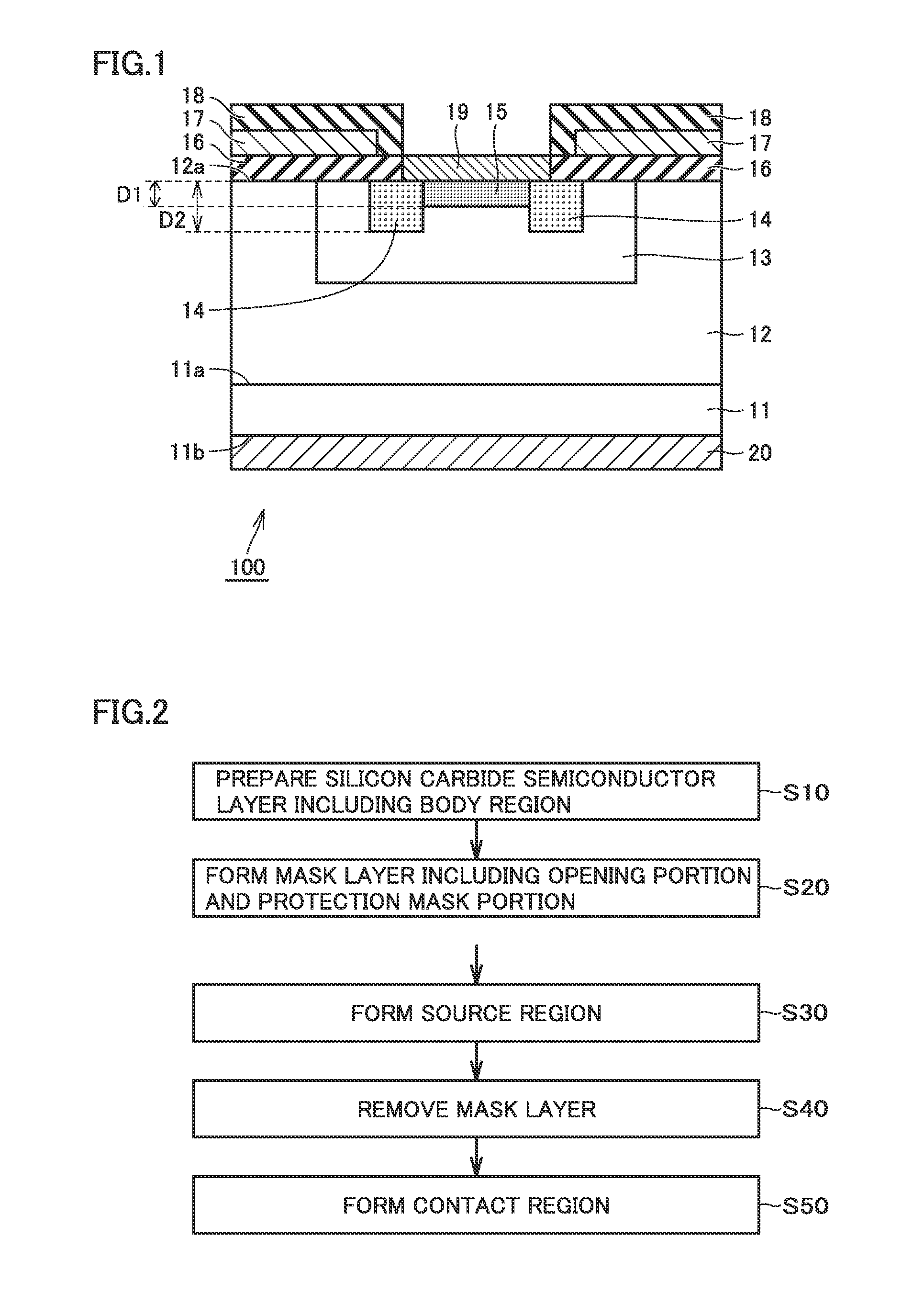
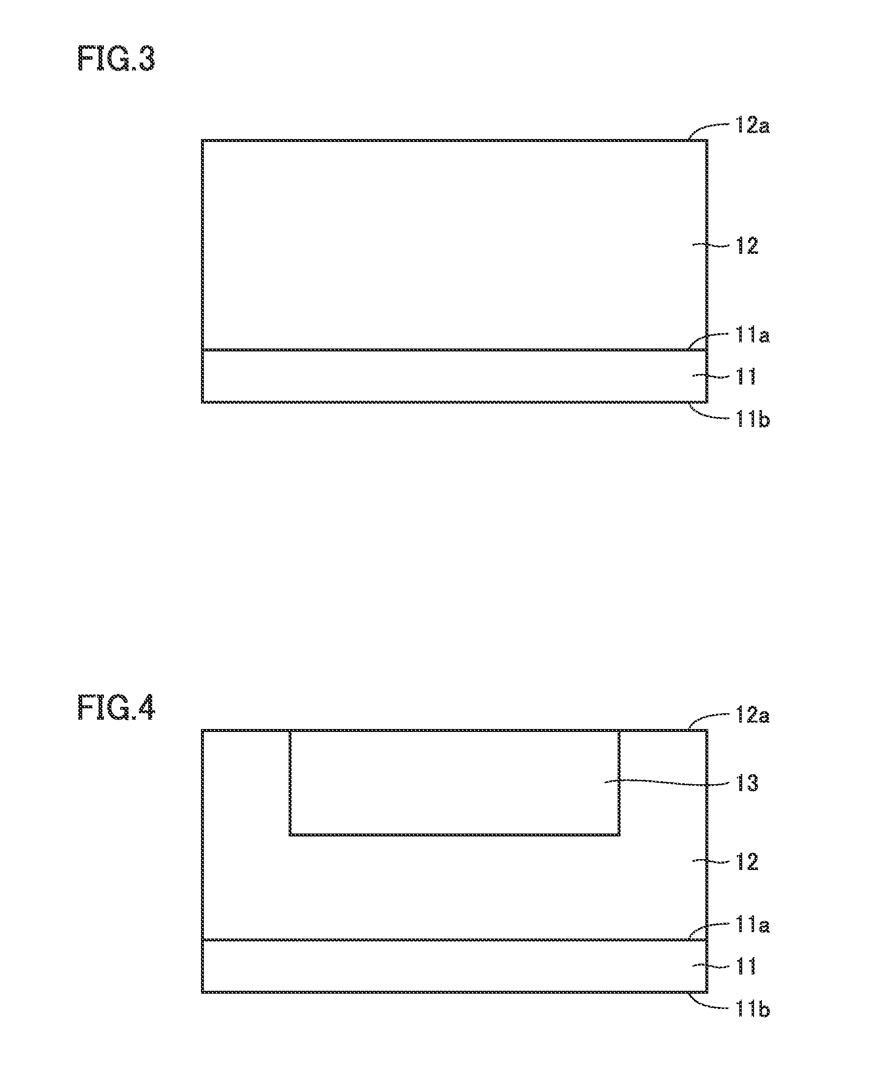
[0053]A structure of a silicon carbide semiconductor device 100 according to a first embodiment will initially be described with reference to FIG. 1. Silicon carbide semiconductor device 100 according to the first embodiment is implemented as a planar MOSFET. Silicon carbide semiconductor device 100 includes an epitaxial substrate 10, a gate oxide film 16, a gate electrode 17, an interlayer insulating film 18, a source electrode 19, and a drain electrode 20. Epitaxial substrate 10 includes a base substrate 11, silicon carbide semiconductor layer 12, body region 13, source region 14, and p+ contact region 15.

[0054]Base substrate 11 is composed of single-crystal silicon carbide having hexagonal crystal system and have an n conductivity type (the second conductivity type). Base substrate 11 contains an impurity such as N (nitrogen) at a high concentration. A concentration of an impurity such as nitrogen contained in base substrate 11 is, for example, around 1.0×1018 cm−3. Base substrat...

second embodiment

[0090]A silicon carbide semiconductor device and a method of manufacturing the same according to a second embodiment will now be described with reference to FIGS. 1 and 15 to 17. Though the silicon carbide semiconductor device according to the second embodiment is basically the same in feature as the silicon carbide semiconductor device and the method of manufacturing the same according to the first embodiment, it is different in that n-type region 14A is not formed in a region where p+ contact region 15 is to be formed in the step of forming source region 14 (S30) in the method of manufacturing a silicon carbide semiconductor device, that is, different in that p+ contact region 15 is formed by implanting ions of a p-type impurity into p body region 13, rather than by forming p+ contact region 15 as replacement for n-type region 14A by implanting ions of a p-type impurity into n-type region 14A in the step of forming p+ contact region 15 (S50). A construction of the silicon carbide ...


PUM

PropertyMeasurementUnit
total azimuth angleaaaaaaaaaa
thicknessaaaaaaaaaa
thicknessaaaaaaaaaa

Abstract

The silicon carbide semiconductor layer includes a first impurity region, a second impurity region, and a third impurity region. Turning to a first position at which an impurity concentration 1/10 as high as a highest impurity concentration is exhibited in a concentration profile of an impurity having the first conductivity type in a direction perpendicular to the main surface in the third impurity region and a second position at which an impurity concentration 1/10 as high as a highest impurity concentration is exhibited in a concentration profile of an impurity having the second conductivity type in the direction perpendicular to the main surface in the second impurity region, a first depth from the main surface to the first position is shallower than a second depth from the main surface to the second position. The electrode is electrically connected to the second impurity region and the third impurity region.

Description

TECHNICAL FIELD[0001]The present invention relates to a silicon carbide semiconductor device and a method of manufacturing the same, and particularly to a silicon carbide semiconductor device having an ohmic electrode low in contact resistance and a method of manufacturing the same.BACKGROUND ART[0002]From a point of view of lowering in on resistance, a contact resistance between a silicon carbide semiconductor layer and an electrode is preferably lower in a silicon carbide semiconductor device containing silicon carbide (SiC) as a semiconductor material.[0003]In order to lower a contact resistance between the silicon carbide semiconductor layer and the electrode, in general, a contact region high in impurity concentration is formed in the silicon carbide semiconductor layer. For example, when the silicon carbide semiconductor device is implemented as an MOSFET, a well region is formed in the silicon carbide semiconductor layer, and a source region and a contact region in contact wi...

Claims


Application Information

Patent Timeline
Patent Type & Authority Applications(United States)
IPC IPC(8): H01L29/16H01L29/78H01L21/04H01L29/66H01L29/423H01L29/04
CPCH01L29/1608H01L29/4236H01L29/7813H01L21/0465H01L29/66068H01L29/045H01L29/086H01L29/1095H01L29/7802
Inventor MASUDA, TAKEYOSHI
Owner SUMITOMO ELECTRIC IND LTD
Why Eureka
Try Eureka