
Right Angle Transition to Circuit

a right angle transition and circuit technology, applied in the field of circuit design, can solve the problems of poor input match, poor impedance matching, and high return loss of most right angle launches, and achieve the effect of reducing manufacturing variations regarding the distance between the center pin and the ground plan

Active Publication Date: 2016-08-18
NATIONAL INSTRUMENTS
View PDF3 Cites 10 Cited by
  • Summary
  • Abstract
  • Description
  • Claims
  • Application Information

AI Technical Summary

Benefits of technology

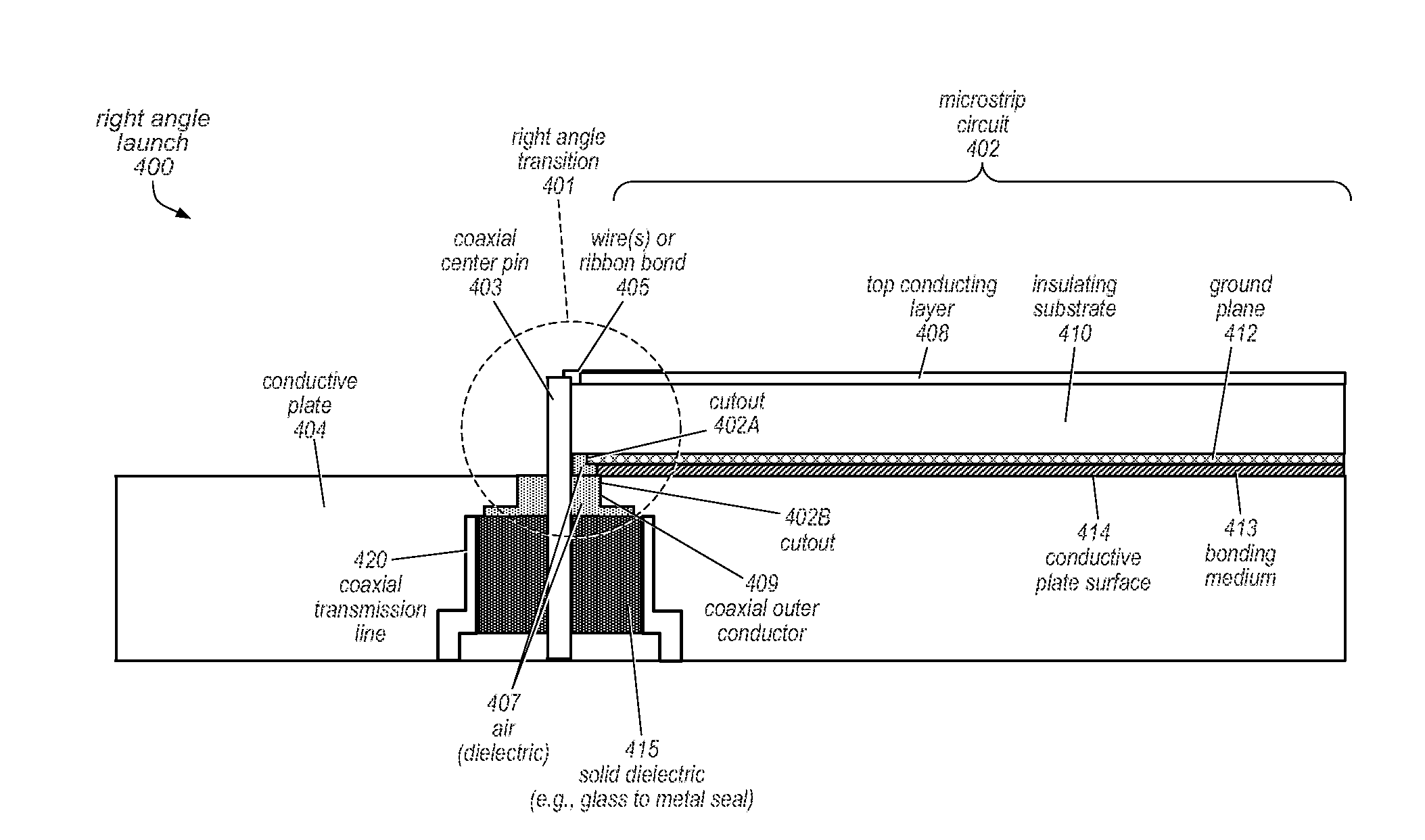
The patent text describes a system that includes a conductive plate, coaxial transmission line, and circuit. The coaxial transmission line has a center pin and an outer conductor with air dielectric between them. The circuit is parallel to the conductive plate and has a top conducting layer, ground plane with a cutout, and an insulating substrate between the top conducting layer and the ground plane, which abuts the center pin of the coaxial transmission line. A right angle transition is used to connect the center pin of the coaxial transmission line to the top conducting layer of the circuit. The cutout helps minimize manufacturing variations and the right angle transition helps tune out inductance. The technical effects of the system include reducing manufacturing variations and improving signal quality.

Problems solved by technology

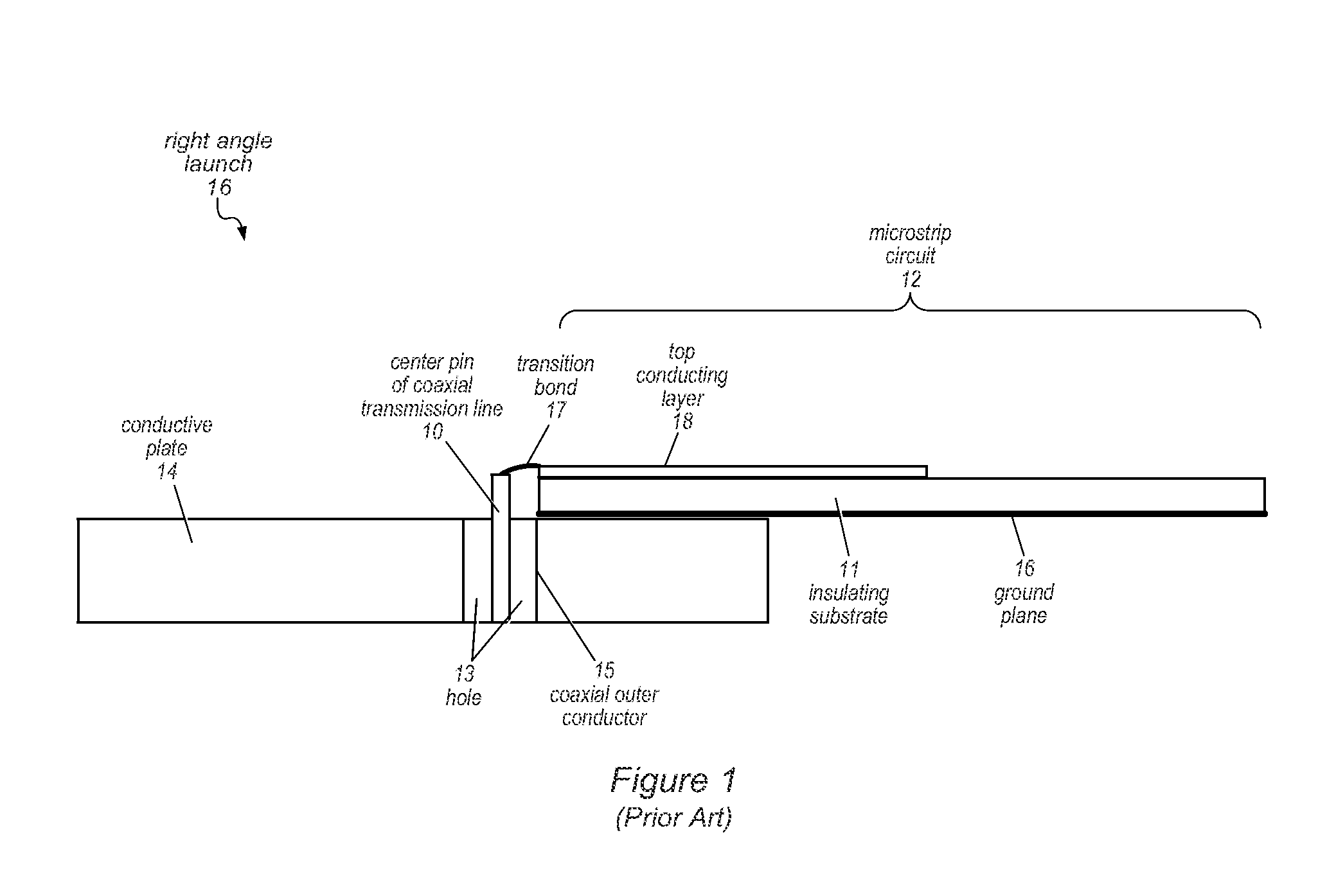
However, most right angle launches have poor input match, e.g., poor impedance matching, referred to as S11 (and possibly other S-Parameters) in the art of linear electrical networks in the RF domain, high return loss, etc.
For example, in many cases, there may be unwanted capacitance produced by the proximity of a coaxial connector center pin, e.g., of an SMP connector of a microcircuit, to the conductive ground plane layer of a microstrip circuit.
Note, for example, that since the center pin of a vertical or orthogonal coaxial connector, such as a subminiature push-on (SMP) connector, is at a right angle with respect to the top conductive layer and the ground plane of the microstrip circuit, the electric and magnetic fields of the coaxial connector are not aligned with those of the microstrip circuit components, and thus, the 90 degree transition between the circuits may further complicate input (e.g., impedance) matching between the circuits.
These discontinuities in the ground currents and the longer conductive transition bond is what makes a right angle (launch) transition so challenging with regards to reliable impedance matching, particularly in mass production.
Said another way, the unwanted capacitance due to discontinuities in the transition gives rise to impedance, and thus impedance mismatching, which produces unwanted signal reflections due to inductance introduced in bonding (transitioning) over from the vertical connector to a horizontal substrate, which becomes progressively more of a problem with increased frequency.
The effects of most attempts to tune out this inductance are limited due to variations in implementation.
For example, tolerances in manufacturing processes often introduce variance in the relative geometry of the circuits to be joined, e.g., variation in the distance between the center pin and the ground plane of the microstrip circuit, with resultant variance in the inductance, which leads to corresponding variations in the impedances, and mismatches thereof.
In other words, due to variations in the proximity that can occur in mass production, i.e., each produced circuit assembly may have a different degree of proximity between the vertical center pin and the ground plane of the microstrip circuit, and thus, different impedance values, which makes impedance matching difficult and unreliable.
Additionally, higher frequencies, e.g., RF, generate greater inductance in the assembly, which also increases impedance, thereby exacerbating impedance matching problems.

Method used


Image

  • Right Angle Transition to Circuit
  • Right Angle Transition to Circuit
  • Right Angle Transition to Circuit

Examples


Embodiment Construction

Terms

[0027]The following is a glossary of terms used in the present application:

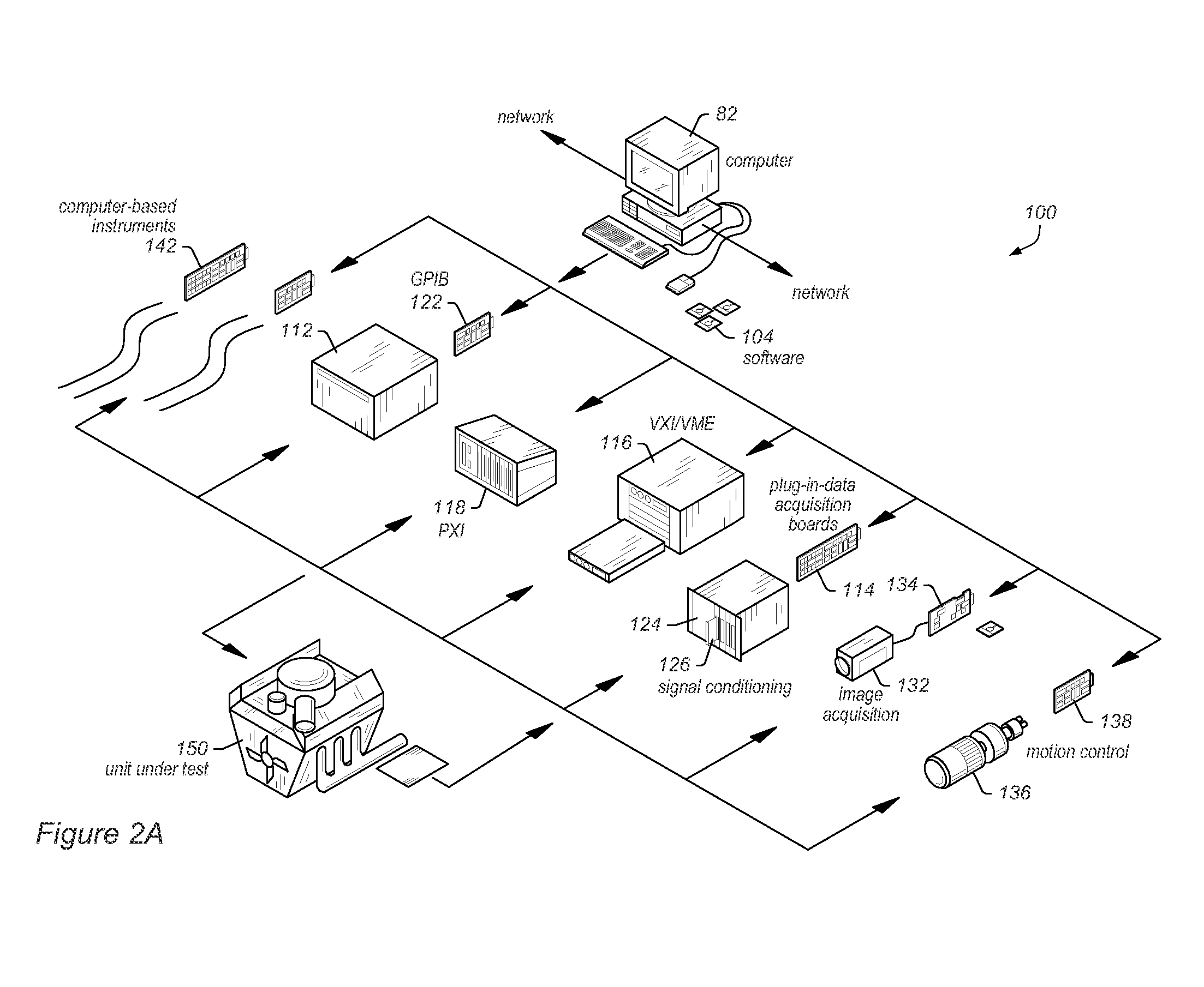
[0028]Memory Medium—Any of various types of non-transitory computer accessible memory devices or storage devices. The term “memory medium” is intended to include an installation medium, e.g., a CD-ROM, floppy disks 104, or tape device; a computer system memory or random access memory such as DRAM, DDR RAM, SRAM, EDO RAM, Rambus RAM, etc.; a non-volatile memory such as a Flash, magnetic media, e.g., a hard drive, or optical storage; registers, or other similar types of memory elements, etc. The memory medium may comprise other types of non-transitory memory as well or combinations thereof. In addition, the memory medium may be located in a first computer in which the programs are executed, or may be located in a second different computer which connects to the first computer over a network, such as the Internet. In the latter instance, the second computer may provide program instructions to the first compu...


PUM


Abstract

Right angle transition to circuit. A system includes a conductive plate, coaxial transmission line, a circuit, parallel to the conductive plate, and a right angle transition from the coaxial transmission line to the circuit. The transmission line includes a center pin protruding through a hole in the plate, an outer conductor formed by a conductive surface of the hole, and air dielectric between. The circuit includes a top conducting layer (TCL), ground plane with cutout, and an insulating substrate between the TCL and ground plane that abuts the pin. The transition includes the pin, a conductive element connecting the center pin to the TCL, the outer conductor, the air dielectric, the abutment of the substrate against the pin, and the cutout. The abutment and cutout minimize manufacturing variations regarding distance between the pin and the ground plane. The transition tunes out inductance introduced by bonding the pin to the TCL.

Description

PRIORITY DATA[0001]This application claims benefit of priority to U.S. Provisional Application Ser. No. 62 / 117,547, titled “Right Angle Transition to Microstrip Circuit”, filed Feb. 18, 2015, whose inventors were Ron J. Barnett and Gregory S. Gonzales, and which is hereby incorporated by reference in its entirety as though fully and completely set forth herein.FIELD OF THE INVENTION[0002]The present invention relates to the field of circuit design, and more specifically, to a right angle transition to a circuit, e.g., for radio frequency (RF) systems.DESCRIPTION OF THE RELATED ART[0003]Many electronic devices include components, e.g., circuits, conductive plates, e.g., housings, and so forth, that must be interconnected to operate, including circuits with surface mount packages where components are mounted on the surface (floor) of a conductive housing or printed circuit board (PCB), and microstrip circuits, e.g., thin film circuits, where layers of material on the order of a nanome...

Claims


Application Information

Patent Timeline
IPC IPC(8): H01P5/08H01P3/08H03H7/38H01P3/06
CPCH01P5/085H03H7/38H01P3/08H01P3/06
Inventor BARNETT, RON J.GONZALES, GREGORY S.
Owner NATIONAL INSTRUMENTS
Learn More