

Scanning probe microscope prober employing self-sensing cantilever
a scanning probe microscope and cantilever technology, applied in scanning probe microscopy, measuring devices, instruments, etc., can solve the problems of increasing the number of devices in which a current is difficult to take out from the backside, the substrate, and the difficulty in not a few cases to take out a current signal from the backside, so as to achieve a small leakage current
- Summary
- Abstract
- Description
- Claims
- Application Information
AI Technical Summary
Benefits of technology
Problems solved by technology
Method used
Image

Examples
embodiment 1
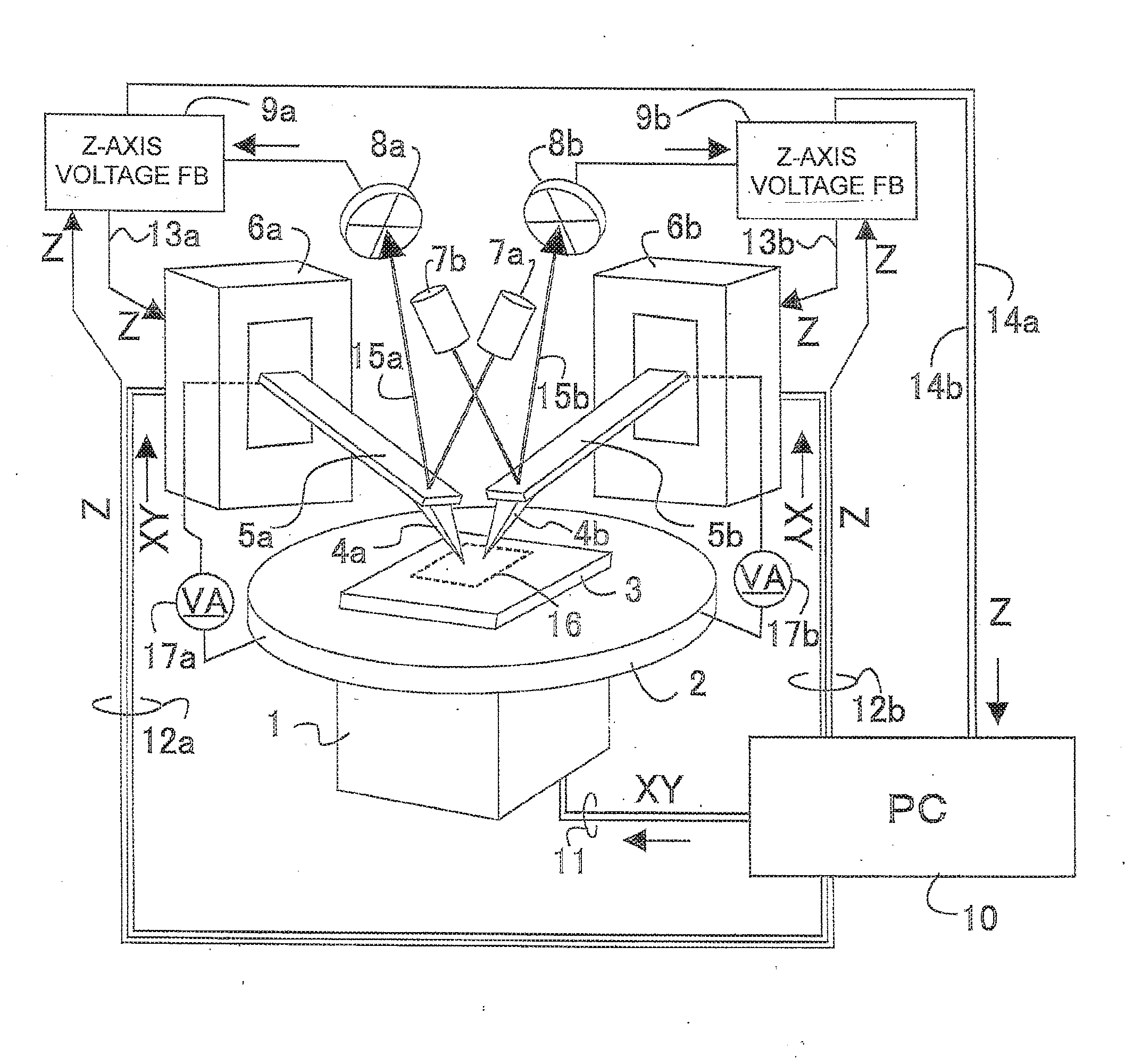
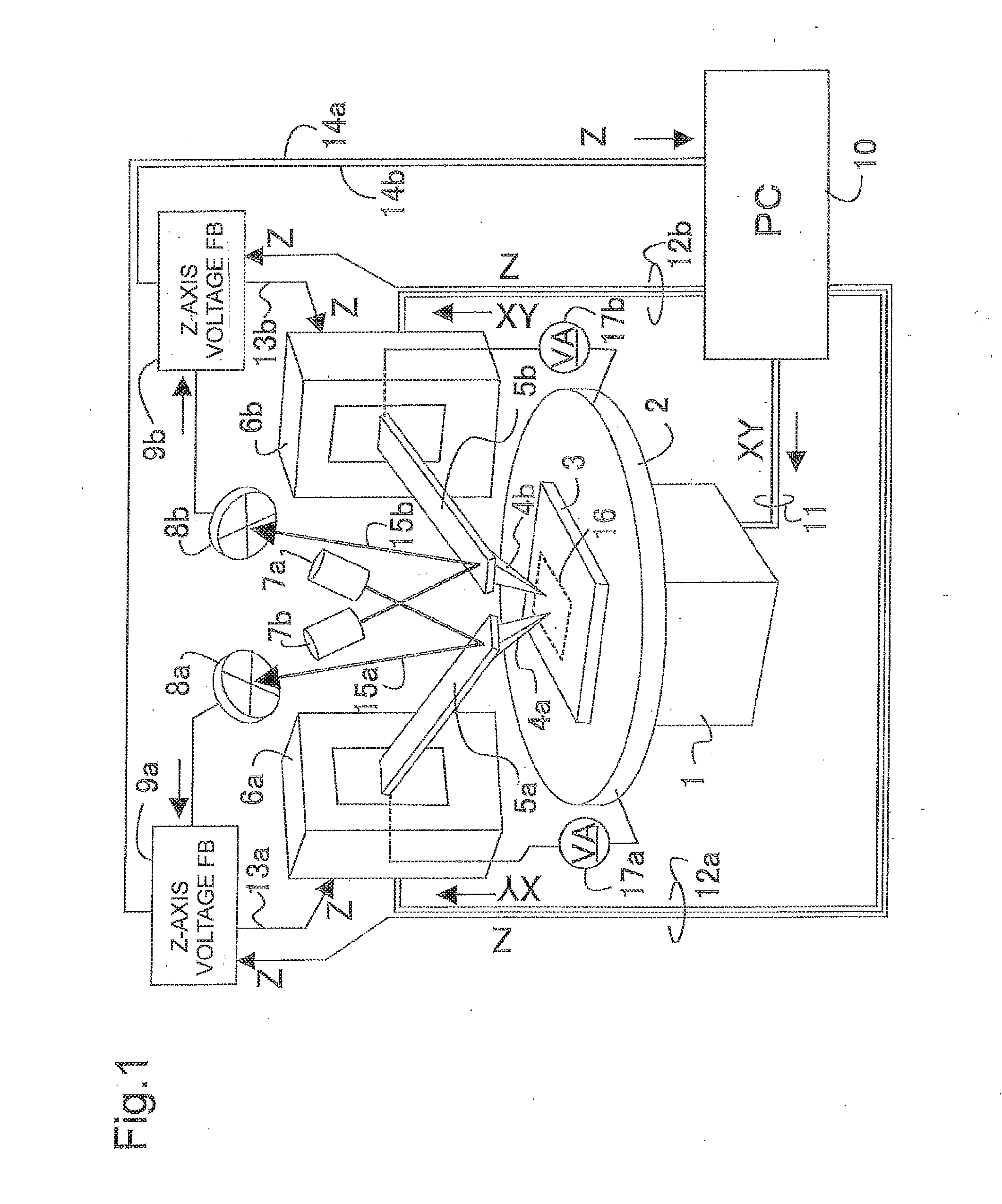
[0050]FIG. 3 is a schematic view of a scanning probe microscope prober using a self-sensing cantilever according to the present invention. It is generally known that there are several operation modes for an SPM, i.e., 1) a contact mode, 2) a noncontact mode, 3) a tapping mode, 4) a force mode, etc. The present invention can be applied to the SPM operating in any of the above modes. FIG. 3 illustrates, as a typical example, a multi-probe scanning probe microscope prober operating in the contact mode and using two AFMs.
[0051]A measurement object 3 is, e.g., a semiconductor chip for which a failure analysis is to be performed, and it is placed on a stage 2. The stage 2 is movable parallel to its surface, and is driven by a driver 1 along X- and Y-axes, which are defined in advance. For the measurement object 3, an AFM image is captured and electrical measurement is performed by employing a cantilever 5a (or 5b) that includes a probe 4a (or 4b). The cantilever 5a (or 5b) is movable by a...
embodiment 2
[0061]The electrical measurements of the measurement object 3 by the above-described scanning probe microscope prober using the self-sensing cantilever, illustrated in FIG. 3, are performed in accordance with the procedures illustrated in FIG. 6, for example.
[0062]1. Several positions are optically checked while the sample stage is moved. These checks are to measure a displacement angle of a sample relative to the sample stage depending on how the sample is placed on the sample stage.
[0063]2. An initial position is checked to set a start point. At this time, an encoder value of the sample stage is reset.
[0064]3. The probe stages are driven with the aid of an optical microscope image for automatically moving the probe tips to come close to each other. The movement of the probe tips in this case can be performed with an error of about 1 micron.
[0065]Here, closed loop control of the sample stage is started.
[0066]4. Mutual positions of the cantilever probes are checked. This check is pe...
embodiment 3
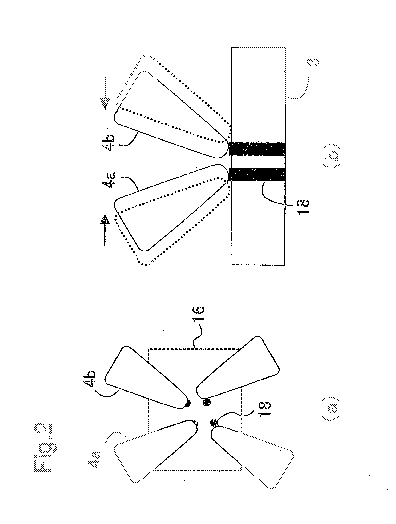
[0081]In above Embodiment, the probes are arranged at positions spaced apart from each other through the predetermined distance by employing an alignment mark or a substitute, or an optical microscope. In the case employing the optical microscope, even when the object has a relatively large size in comparison with the very fine wire, the probe tip is damaged in many cases if the object size is not greater than a limit recognizable by the optical microscope. In view of such a point, damage of the probe tip can be avoided in accordance with the following procedures.
[0082]1) Respective positions of the probes are set such that conduction characteristics between the probes represent the probes being located at positions close to each other. For example, as illustrated in FIG. 9(a), one or both of the probes are moved to come into such a close state as generating flow of a tunnel current or an ion current with ionized gas. It is here important to stop the one or both probes with the aid ...
PUM
 Abstract
Description
Claims
Application Information