Controller, semiconductor memory system and operating method thereof

a memory system and control board technology, applied in the field of semiconductor memory systems and operating methods, can solve the problems of limited voltage window available for threshold voltage distribution, increased read failure rate, and reduced reliability, and achieve the effect of optimizing the read voltage of data stored in the memory cell

Active Publication Date: 2016-08-25
SK HYNIX INC
View PDF6 Cites 14 Cited by
  • Summary
  • Abstract
  • Description
  • Claims
  • Application Information

AI Technical Summary

Benefits of technology

[0018]Various embodiments of the present invention are directed to a controller, a semiconductor memory system, and an operating method thereof capable of precisely determining optimal read voltages for data stored in memory cells.
[0039]In accordance with various embodiments of the present invention, an optimal read voltage for data stored in memory cell of a semiconductor memory device may be effectively determined.

Problems solved by technology

Volatile memory devices lose data stored therein when their power supplies are interrupted, whereas nonvolatile memory devices retain data stored therein even when their power supply is interrupted.
In particular, flash memory devices are widely used as storage mediums in computer systems due to their high program speed, low power consumption and large data storage capacity.
However, as the number of bits programmed in each memory cell increases, reliability decreases and read failure rates increase.
However, the voltage window available for threshold voltage distributions is limited.
This charge loss may accelerate when the tunnel oxide film deteriorates from numerous program and erase operations.
Charge loss results in a decrease in the threshold voltages of memory cells.
Further, program disturbance, erase disturbance and / or back pattern dependency also cause increases in threshold voltages.
Once threshold voltage distributions overlap, read data may have a significant number of errors when a particular read voltage is applied to a selected word line.
However, when threshold voltage distributions overlap, the memory cell, which actually has the third program state ‘P3’, may be erroneously determined to have the second program state ‘P2’.
In short, when the threshold voltage distributions overlap as illustrated in FIG. 2, read data (i.e. data which is read from a memory cell) may include a significant number of errors.

Method used


Image

  • Controller, semiconductor memory system and operating method thereof
  • Controller, semiconductor memory system and operating method thereof
  • Controller, semiconductor memory system and operating method thereof

Examples


Embodiment Construction

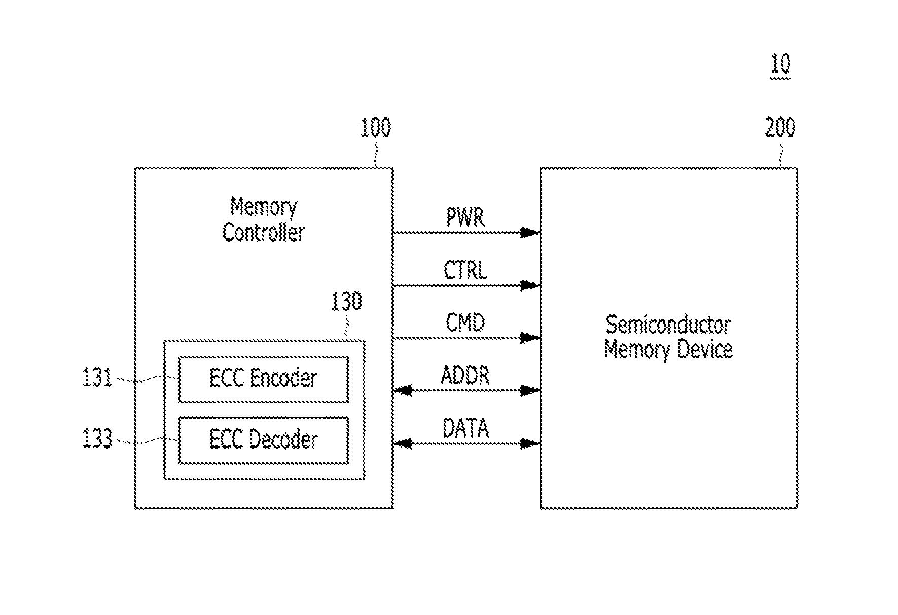
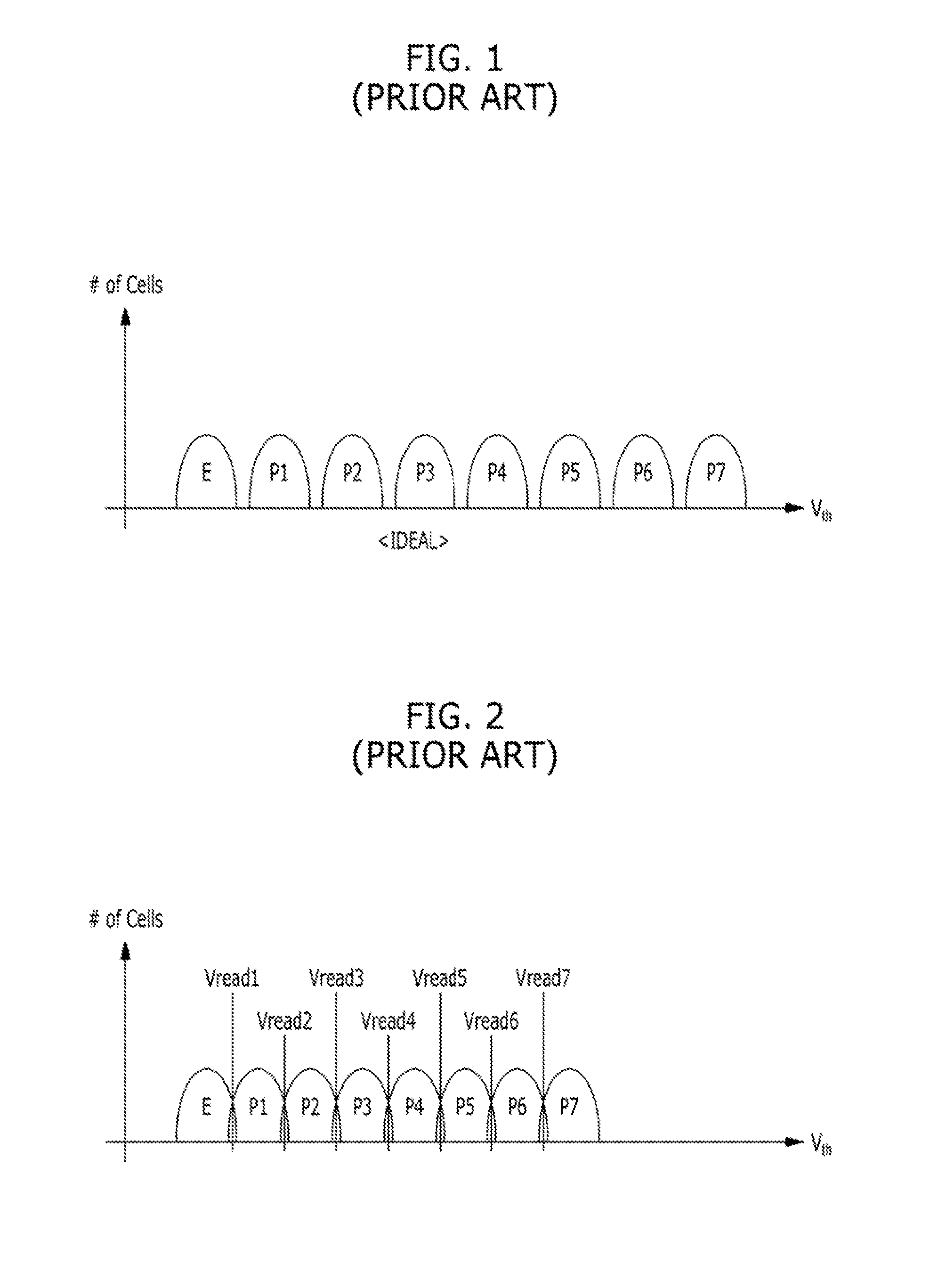
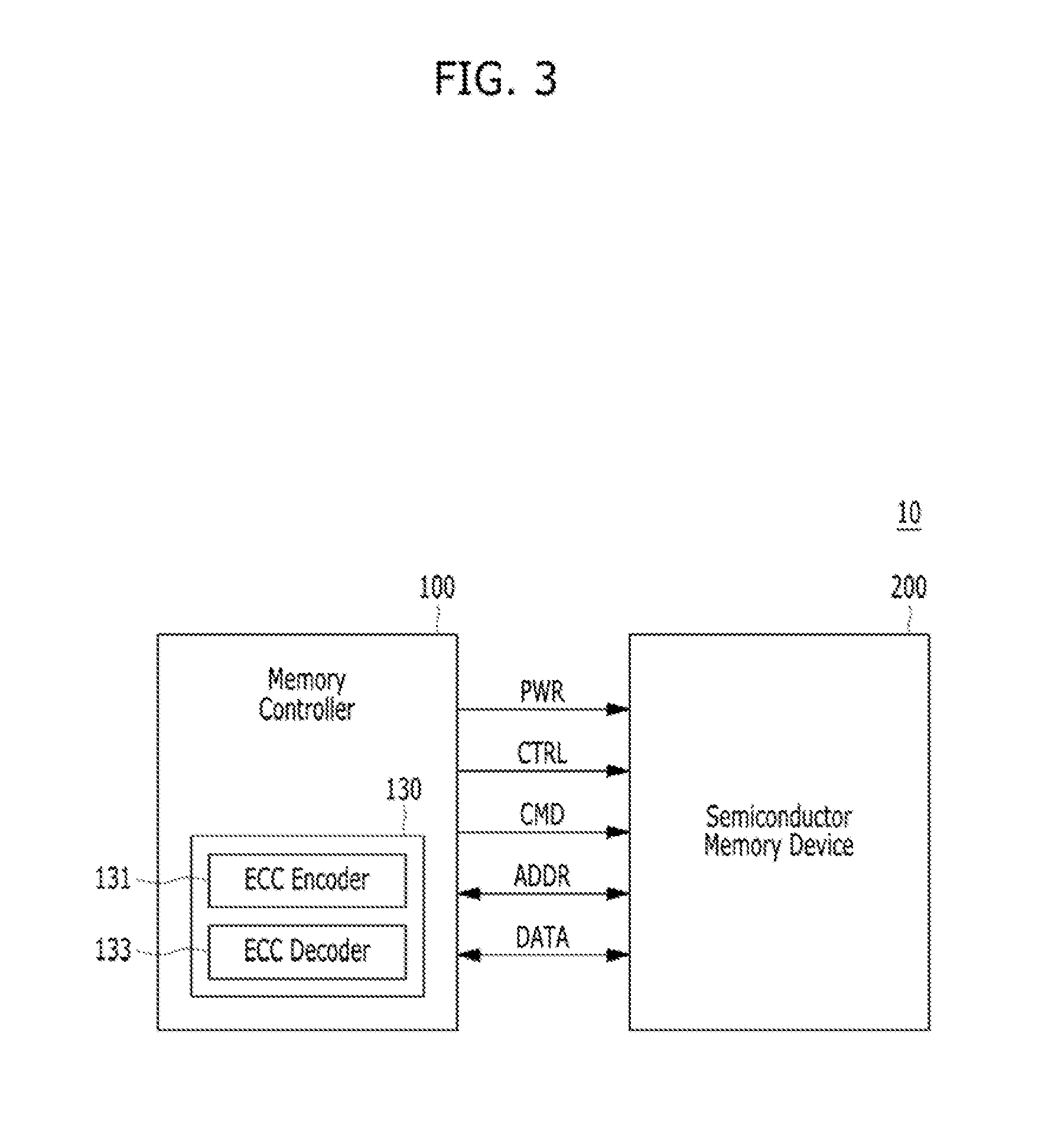
[0062]Various embodiments will be described below in more detail with reference to the accompanying drawings. The present invention may, however, be embodied in different forms and should not be construed as limited to the embodiments set forth herein. Rather, these embodiments are provided so that this disclosure will be thorough and complete and will fully convey the scope of the present invention to those skilled in the art. The drawings are not necessarily to scale and, in some instances, proportions may have been exaggerated in order to clearly illustrate features of the embodiments. Throughout the disclosure, reference numerals correspond directly to the like parts in the various figures and embodiments of the present invention. It is also noted that in this specification, “connected / coupled” refers to one component not only directly coupling another component but also indirectly coupling another component through an intermediate component. In addition, a singular form may inc...


PUM


Abstract

An operating method of a controller that includes: when a first ECC decoding on data read from a semiconductor memory device according to a hard read voltage fails, generating one or more quantization intervals based on the number of unsatisfied syndrome check (USC), which is a result of the first ECC decoding; and performing a second ECC decoding on the data by generating soft read data according to soft read voltages determined by the hard read voltage and the quantization intervals.

Description

CROSS-REFERENCE TO RELATED APPLICATIONS[0001]The present application claims priority of Korean Patent Application No. 10-2015-0025192, filed on Feb. 23, 2015, which is incorporated herein by reference in its entirety.BACKGROUND[0002]1. Field[0003]Various exemplary embodiments of the present invention relate to a semiconductor design technology and, more particularly, to a controller, a semiconductor memory system, and an operating method thereof.[0004]2. Description of the Related Art[0005]Semiconductor memory devices are generally classified into volatile memory devices, such as Dynamic Random Access Memory (DRAM) and Static RAM (SRAM), and nonvolatile memory devices, such as Read Only Memory (ROM), Mask ROM (MROM), Programmable ROM (PROM), Erasable PROM (EPROM), Electrically EPROM (EEPROM), Ferromagnetic RAM (FRAM), Phase change RAM (PRAM), Magnetoresistive RAM (MRAM), Resistive RAM (RRAM) and flash memory.[0006]Volatile memory devices lose data stored therein when their power sup...

Claims


Application Information

Patent Timeline
Patent Type & Authority Applications(United States)
IPC IPC(8): G06F11/10G11C16/26H03M13/15G11C29/52H03M13/11
CPCG06F11/1068G11C29/52G11C16/26H03M13/1575H03M13/1102G11C11/5642G11C2029/0411H03M13/6325G06F11/1012H03M13/3707H03M13/3746G11C16/04G11C16/34G11C29/024G11C29/14G11C29/42G11C2211/5614H03M13/1515H03M13/152H03M13/23H03M13/251H03M13/256H03M13/2957
Inventor KIM, JAE-BUM
Owner SK HYNIX INC
Why Eureka
Try Eureka