Color display device

a color display device and color technology, applied in the field of display technology, can solve the problems of low efficiency of display device, low productivity and cost, color shifting of color display device, etc., and achieve the effect of simple manufacturing technique, reduced cost and extended lifespan

Active Publication Date: 2016-09-01
SHENZHEN CHINA STAR OPTOELECTRONICS TECH CO LTD
View PDF4 Cites 1 Cited by
  • Summary
  • Abstract
  • Description
  • Claims
  • Application Information

AI Technical Summary

Benefits of technology

[0020]The efficacy of the present invention is that the present invention provides a color display device, which uses an arrangement of a white light emission layer and a color change layer to make the color display device emitting various colors of light. The white light emission layer is formed through a thermal evaporation process so that there is no need of a fine metal mask in a manufacturing process, making the manufacturing technique simple and the cost reduced. Quantum dot materials are used to make color filter layers of the color change layer so as to take advantage of the advantages of stabilization of perform

Problems solved by technology

However, due to the requirement of masks of high precision and alignment of high accuracy in making high resolution display screens, the productivity is relatively low and the cost is high.
Further, due the great difference in respect of lifespan, excitability, and degree of attenuation among the three primary colors, color shifting of a color display device may result.
However, si

Method used


Image

  • Color display device
  • Color display device
  • Color display device

Examples


Embodiment Construction

[0028]To further expound the technical solution adopted in the present invention and the effectiveness thereof, a detailed description will be given to a preferred embodiment of the present invention and the attached drawings.

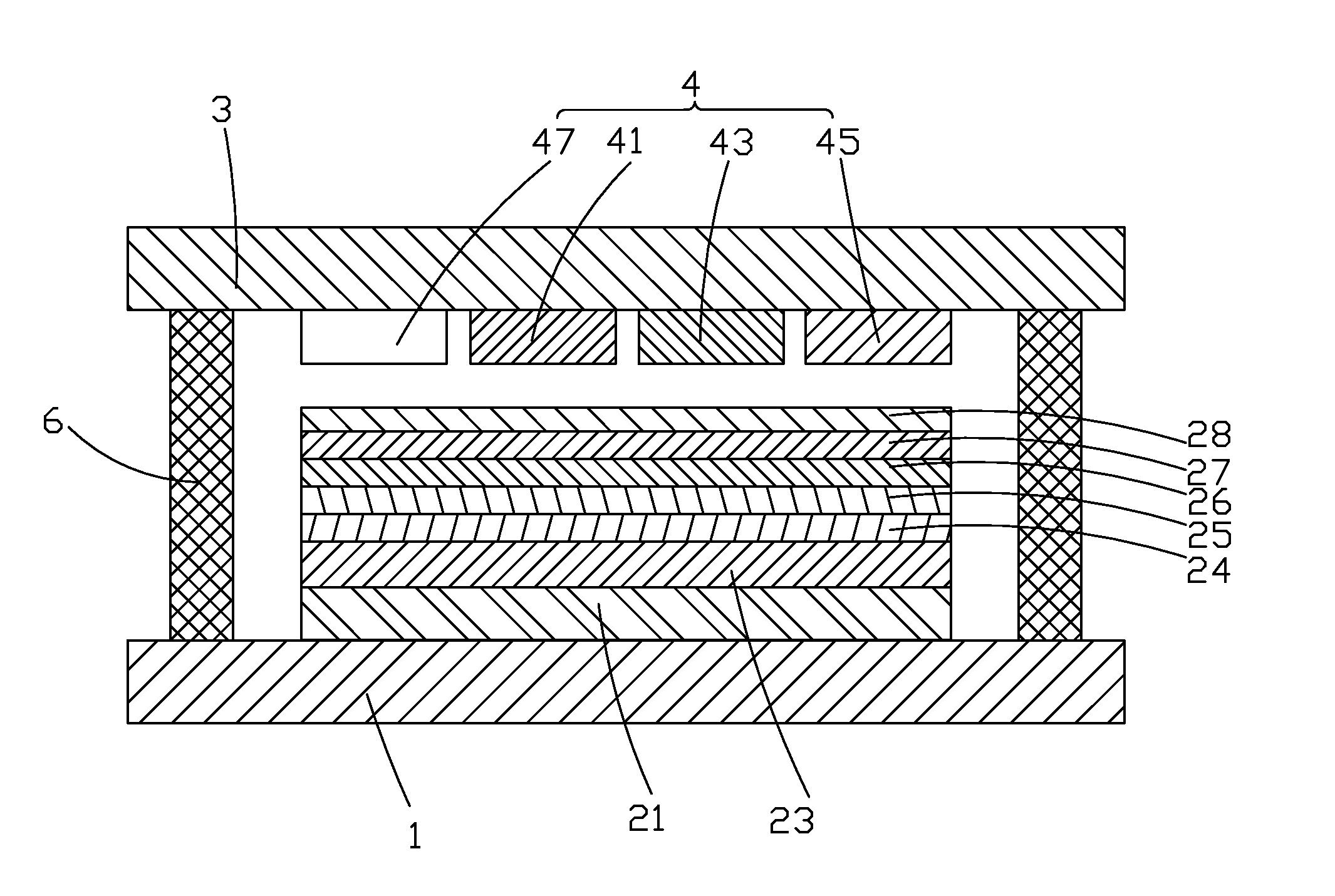
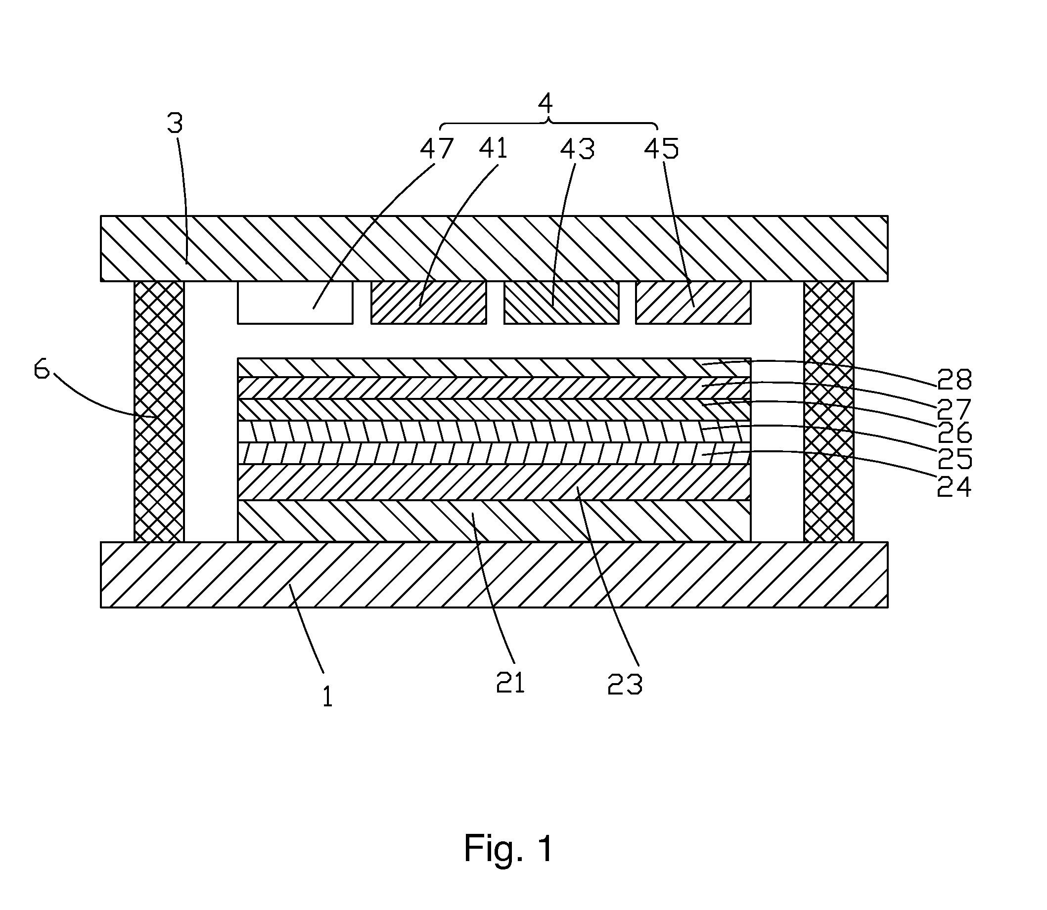
[0029]Referring to FIG. 1, the present invention provides a color display device, which comprises a substrate 1, an anode 21 formed on the substrate 1, a thin-film transistor (TFT) array 23 formed on the anode 21, a hole injection layer 24 formed on the TFT array 23, a hole transporting layer 25 formed on the hole injection layer 24, a white light emission layer 26 formed on the hole transporting layer 25, an electron transporting layer 27 formed on the white light emission layer 26, a cathode 28 formed on the electron transporting layer 27, a cover plate 3 disposed above the cathode 28 and bonded to the substrate 1, a color change layer 4 formed on an inside surface of the cover plate 3, and a sealing enclosure resin 6 bonding the substrate 1 and the cover pla...


PUM

PropertyMeasurementUnit
Flexibilityaaaaaaaaaa

Abstract

The present invention provides a color display device, including a substrate, an anode formed on the substrate, a TFT array formed on the anode, a hole injection layer formed on the TFT array, a hole transporting layer formed on the hole injection layer, a white light emission layer formed on the hole transporting layer, an electron transporting layer formed on the white light emission layer, a cathode formed on the electron transporting layer, a cover plate disposed above the cathode and bonded to the substrate, a color change layer formed on an inside surface of the cover plate, and a sealing enclosure resin bonding the substrate and the cover plate together, wherein the color change layer includes a blue sub-pixel zone, a green sub-pixel zone, a red sub-pixel zone, and a white sub-pixel zone that are spaced from each other, the blue sub-pixel zone including a blue light filter layer formed therein, the green sub-pixel zone including a green light filter layer or a green light change layer formed therein, the red sub-pixel zone including a red light filter layer or a red light change layer formed therein, the white sub-pixel zone comprising no filter layer formed therein.

Description

BACKGROUND OF THE INVENTION[0001]1. Field of the Invention[0002]The present invention relates to the field of displaying technology, and in particular to a color display device.[0003]2. The Related Arts[0004]An OLED (Organic Light-Emitting Diode) is a flat panel displaying technique of extremely prosperous future and it shows excellent displaying performance and also possesses various advantages, such as being self-luminous, simple structure, being ultra-thin, fast response, wide view angle, low power consumption, and being capable of achieving flexible displaying and is thus regarded as a “dream display”. In addition, the investment of manufacturing installation is far less than that of liquid crystal displays so that it has attracted the attention of major display manufacturers and becomes the mainstream of the third-generation display devices of the field of displaying technology.[0005]Heretofore, several technical passageways have been proposed to achieve coloring of OLEDs, one ...

Claims


Application Information

Patent Timeline
IPC IPC(8): H01L27/32H01L51/00H01L51/52
CPCH01L27/3213H01L51/0081H01L51/5246H01L27/322H01L51/0008H01L2251/5369H01L2251/301H01L2251/5338H01L51/5072H01L51/5056H01L51/5088H01L51/56H01L27/1214H01L51/0061H01L51/0072H01L51/0067H01L51/0085H01L51/0054H01L51/0037H01L51/0035H01L27/3262G02B5/201G02B5/206H10K59/351H10K59/38H10K59/12H10K50/125H10K50/8426H10K59/1213H10K71/16H10K50/15H10K50/16H10K50/17H10K71/00H10K85/111H10K85/324H10K85/342H10K85/622H10K85/636H10K85/654H10K85/1135H10K85/6572H10K2102/00H10K2102/311H10K2102/331
Inventor LIU, YAWEIWANG, YIFAN
Owner SHENZHEN CHINA STAR OPTOELECTRONICS TECH CO LTD
Why Eureka
Try Eureka