Low-power APD bias controller, bias control method, and photoelectric receiver

a low-power, bias controller technology, applied in the field of optical communication, can solve the problems of large power waste, large power consumption, and large power consumption of current-limiting resistors, and achieve the effect of sufficient dynamic response capability, maximum signal-to-noise ratio, and low power consumption

Active Publication Date: 2016-09-22
INNOLIGHT TECHNOLOGY PTE LTD
View PDF17 Cites 21 Cited by
  • Summary
  • Abstract
  • Description
  • Claims
  • Application Information

AI Technical Summary

Benefits of technology

[0008]Embodiments of the present disclosure may provide an APD bias control method and a corresponding device that can solve the aforementioned problems and is low in power consumption and high in dynamic response speed.
[0027]APD bias controllers and APD photoelectric receivers designed with the low-power APD bias control method of embodiments of the present disclosure may have the following advantages.
[0028]There may be no damage to the APD with strong optical input. The bias circuit may remain low in power consumption within its nominal optical input power range. The APD may have sufficient dynamic response capability to prevent link interruption caused by photocurrent underload or overload. The APD bias voltage can be precisely adjusted to obtain maximum signal-to-noise ratio and increase the sensitivity level. Temperature compensation can be achieved for the APD bias voltage.

Problems solved by technology

In this patent, a serially connected resistor is used for the bias voltage, and the output voltage of the step-up circuit does not automatically adjust based on the level of the APD photocurrent; when the photocurrent approaches the overload point, the output power is relatively high, and most of the power is wasted on the current-limiting resistor.
In multichannel APD applications, the waste of power is even greater.
In this patent, APD protection is provided through adjustment of the bias voltage by electrical current feedback; it has a small dynamic range and may not play a protective role.
The response time through the DC / DC step-up circuit is usually 0.1 ms-10 ms; when the optical input power increases instantaneously in a time period shorter than the response time of the DC / DC step-up circuit, photocurrent overload and TIA bit errors will occur, and the APD / TIA may be damaged by the overload.

Method used


Image

  • Low-power APD bias controller, bias control method, and photoelectric receiver
  • Low-power APD bias controller, bias control method, and photoelectric receiver
  • Low-power APD bias controller, bias control method, and photoelectric receiver

Examples


embodiment 1

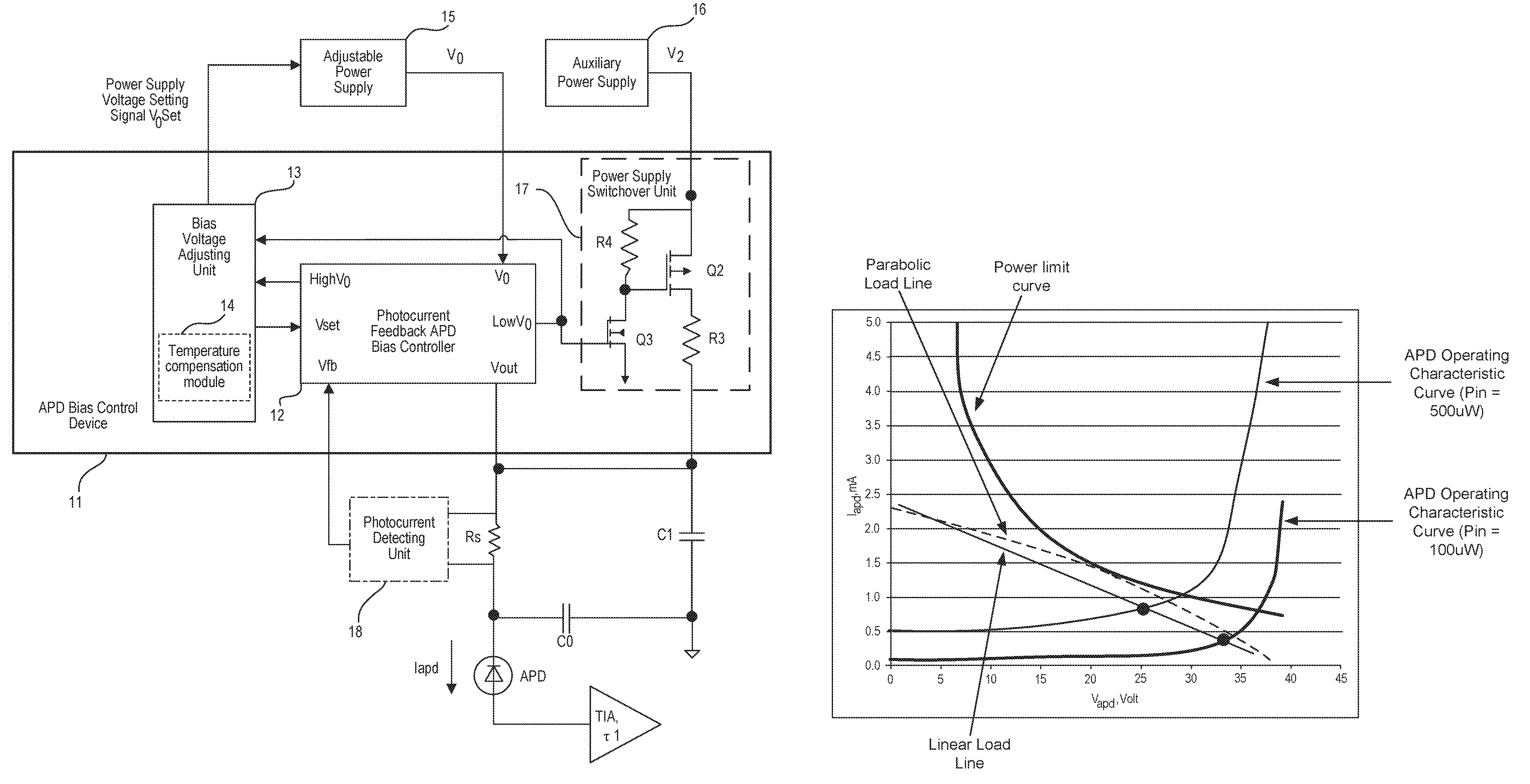
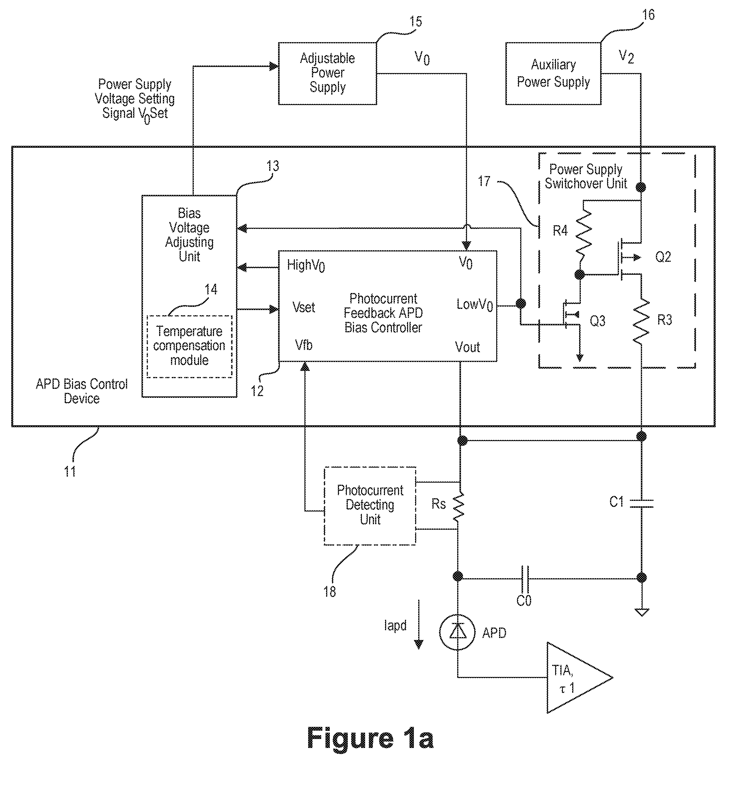
[0053]Let there be an APD, Vbr=+40V, n=2. Further, let Vin=+0.8V; Vs can be neglected; the gain of the sampling circuit (Rs*Gs) is 0.5 k ohm; and the APD responsiveness η=1 mA / mW. Set V0=+40V, and select a linear function for func(x), i.e.

func(Vf)=32*Vfb+0.5=16e3*Iapd+0.5  (8)

Vapd=40−0.8−Vdrop=38.7−16 k*Iapd  (9)

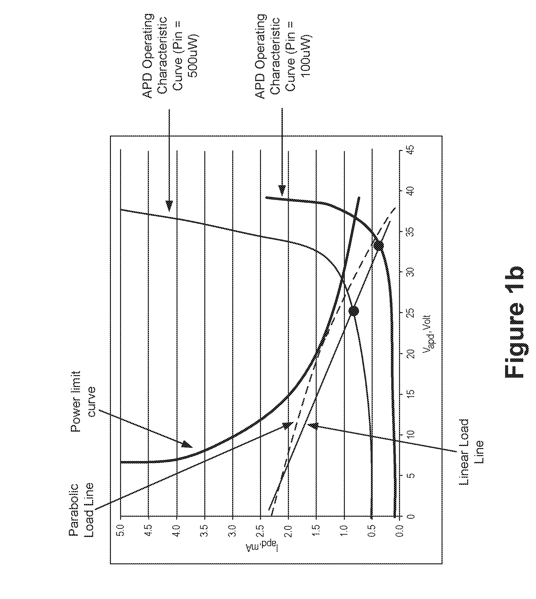
[0054]As shown in FIG. 1b, we can draw the APD load line (a straight line in this case) in an I-V graph according to Formula 9; on the other hand, we can draw the APD operating characteristic curves at optical input powers of 100 uW and 500 uW, respectively, according to Formula 3. In the I-V graph, the voltage and photocurrent at the point of intersection between the APD operating characteristic curve and the load line are the APD's bias voltage and photocurrent at the corresponding input optical power.

[0055]Let the sensitivity level be Pin=3.8 uW, it can be determined that at this point Iapd=40 uA according to the I-V graph, Vdrop=1.14V and Vapd=38.06V according to Formula...

embodiment 2

[0086]Using the same APD characteristic parameters and circuit parameters in Embodiment 1, and let the sensitivity target be 3.8 uW and func(x) be a linear increasing function determined by Formula 5, i.e., func(Vfb)=16 k*Iapd+0.5, and let B=32, Vset0=Vref=+1.25V, A=32, V0set0=V0 / A=1.25V. Further, let Vdrop0=0.82V, Vdrop_min=Vdrop_extreme=0.5V, Vdrop_max=1.14V. Below is a description of the operating mode of the Vdrop control loop when the optical input power increases from the sensitivity point of 3.8 uW (corresponding Iapd=40 uA) to +1.94 mW (corresponding Iapd=2 mA).

[0087]According to calculations in Embodiment 1, when the optical input power is 3.8 uW and Vdrop is not controlled, according to the load line and characteristic curve shown in FIG. 1b, Iapd=40 uA, Vapd=38.06V, Vdrop=1.14V. After the Vdrop control loop is enabled, because Vdrop is greater than its target value 0.82V, the error integrator will increase ΔV gradually in the negative direction until ΔV=(0.82−1.14) / B=−0.3...

embodiment 3

[0119]Let the APD characteristic parameters, circuit parameters, and Vdrop function be the same as in Embodiment 2. Set R3=16 k ohm, according to the calibration steps described before and Formulas 22 and 25, V0set_opt=1.25V, C=0.5V, V2=40−0.5=39.5V. Further, let the stabilization time of the Vdrop control loop be approximately 500 ms, the current optical input power Pin=1.95 mW, Iapd stabilized at 2 mA, Vdrop control loop stabilized, Vdrop=0.82V, V0=8.32V. The table below describes the process of change in the circuit's operating state when the optical power decreases to the sensitivity point Pin=3.8 uW within 10 us.

Table 1:

[0120]

State of loadState of dual-sourceState of controlTimeOptical powerState of APDcircuitpower supplyloop0 1.95 mWIapd = 2 mA,V0 = 8.32 V,State 1,LowV0 = 0,Vapd = 6.8 V,Vdrop = 0.82 VV2 = 39.5 V,ΔV = −0.99,M = 1.029Vapd1 = 7.82 VVset = 0.26,Continues1.918 mWIapd = 1.98 mA,V0 remains theSeamless switchoverLowV0 = 1,Vapd = 7.02 V,same Vdrop =into State 2.2,ΔV, V...


PUM


Abstract

An avalanche photodiode (APD) bias control method may include acquiring a photocurrent intensity voltage and generating a control signal by superposing the acquired photocurrent intensity voltage and a bias setting signal, wherein the control signal controls a voltage drop between an adjustable power supply output voltage and a voltage of the APD. The APB bias control method may further include adjusting the adjustable power supply output voltage and the bias setting signal simultaneously so that the voltage drop is within a target voltage drop range and the APD bias voltage approaches a bias voltage that corresponds to an APD optical input power. An avalanche photodiode (APD) bias controller and an avalanche photodiode (APD) photoelectric receiver are also provided.

Description

CROSS-REFERENCE TO RELATED APPLICATION[0001]This application claims the benefit of priority to Chinese Application No. CN 201510113780.5, filed Mar. 16, 2015.FIELD OF THE DISCLOSURE[0002]The present disclosure relates to the field of optical communication and, more specifically, the field of low-power APD (avalanche photodiode) bias controllers, APD bias control methods, and APD photoelectric receivers.BACKGROUND[0003]Patent 1 and Patent 2, which disclose technologies relevant to APD bias controllers, are described below.[0004]Patent 1 (Chinese Patent Publication No.: CN1790946A) discloses an optical receiving module with overload protection for use in optical fiber communication. It comprises an avalanche photodiode, a DC / DC step-up circuit that provides a reverse bias voltage to the avalanche photodiode, and a sampling resistor for optical input detection; one end of the sampling resistor is connected to the output end of the DC / DC step-up circuit, a current-limiting protective re...

Claims


Application Information

Patent Timeline
Patent Type & Authority Applications(United States)
IPC IPC(8): G01J1/02G01J1/44
CPCG01J1/0228G01J1/0252G01J2001/4466G01J2001/444G01J1/44H04B10/6911H01L31/02027
Inventor WANG, XIANGZHONG
Owner INNOLIGHT TECHNOLOGY PTE LTD
Why Eureka
Try Eureka