

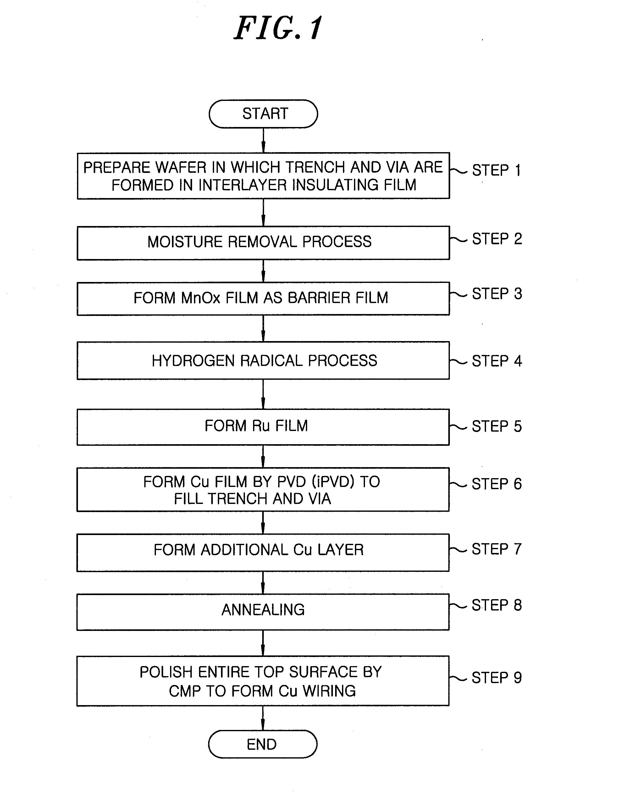
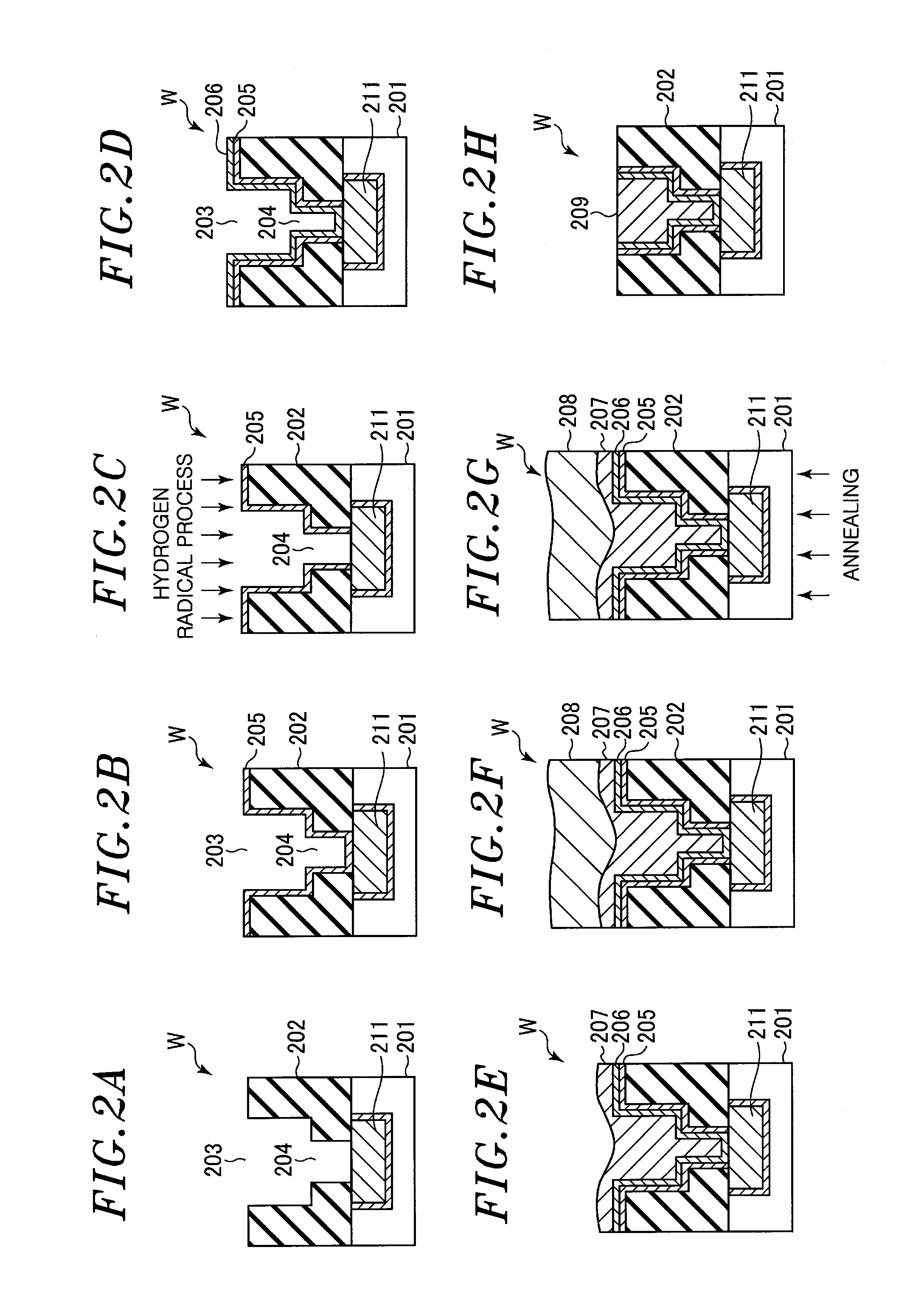
METHOD OF MANUFACTURING Cu WIRING
- Summary
- Abstract
- Description
- Claims
- Application Information
AI Technical Summary
Benefits of technology
Problems solved by technology
Method used
Image

Examples
experiment 1
[0132]In this experiment, a SiOC film was formed as a low-k film on a silicon wafer, a trench was formed in a pattern having a line / space of 60 nm / 60 nm, a MnOx film was formed (with film thickness set to 2.1 nm) by ALD of 30 cycles at 130° C. by using an amide amino alkane-based manganese compound as an organic Mn compound and using H2O (water vapor) as an oxygen-containing gas, the hydrogen radical process was performed for 300 seconds at 300° C. by using remote plasma, a Ru film was formed (with film thickness set to 3.3 nm) by CVD for 300 seconds at 175° C. by using ruthenium carbonyl, and a Cu film was formed (with film thickness set to 150 nm) by iPVD at 300° C. to fill Cu in the trench. Cross-section TEM pictures for this sample are shown in FIG. 19. From FIG. 19, it has been found that the Ru film can be formed as a thin continuous film having a smooth surface state, thereby obtaining a very satisfactory Cu fillability.
experiment 2
[0133]In this experiment, a SiOC film was formed as a low-k film on a silicon wafer, a trench was formed in a pattern having a line / space of 60 nm / 60 nm, a MnOx film was formed (with film thickness set to 1.5 or 2.1 nm) by ALD of 21 or cycles at 130° C. by using an amide amino alkane-based manganese compound as an organic Mn compound and using H2O (water vapor) as an oxygen-containing gas, the hydrogen radical process was performed for 300 seconds at 300° C. or 400° C. by using remote plasma, a Ru film was formed (with film thickness set to 2.9 or 3.8 nm) by CVD for 80 or 120 seconds at 195° C. by using ruthenium carbonyl, and a Cu film was formed (with film thickness set to 150 nm) by iPVD at 300° C. to fill Cu in the trench. In this way, samples A, B and C were prepared. The conditions of forming each sample were as follows.
[0134]
[0135]ALD cycle number for MnOx film: 30 (set film thickness: 2.1 nm)
[0136]Processing temperature of hydrogen radical process: 300° C.
[0137]Film-forming ...
experiment 3
[0147]In this experiment, a SiO2 film was formed on a silicon wafer by CVD using TEOS as an interlayer insulating film, a pattern for electrical characteristics was formed with a line / space of 60 nm / 60 nm, a MnOx film was formed as a barrier film by ALD at 130° C. by using an amide amino alkane-based manganese compound, the hydrogen radical process was performed with a hydrogen concentration of 10.6% for 300 seconds at a certain temperature by using remote plasma of 2 kW, and then a Ru film was formed by CVD using ruthenium carbonyl. subsequently, Cu was filled by iPVD at 300° C. and CMP was performed to form a Cu wiring pattern for electrical characteristics. The conditions of forming the Cu wiring were the following #1 to #6.
[0148]
[0149]ALD cycle number for MnOx film: 30 (set film thickness: 2.1 nm)
[0150]Processing temperature of hydrogen radical process: 300° C.
[0151]Film-forming temperature of Ru film: 175° C.
[0152]Film-forming time of Ru film: 300 sec (set film thickness: 2.7 n...
PUM
 Abstract
Description
Claims
Application Information