
Display panel, driving method thereof, and display device

a technology of display panel and driving method, applied in the field of display technology, can solve the problems of low production yield of array substrate, degradation of display effect, effective area available, etc., and achieve the effects of simple manufacturing process, simple structure and higher transmittan

Active Publication Date: 2016-09-29
BOE TECH GRP CO LTD +1
View PDF5 Cites 3 Cited by
  • Summary
  • Abstract
  • Description
  • Claims
  • Application Information

AI Technical Summary

Benefits of technology

The present invention provides a display panel that has both display and touch control functions, resulting in a simpler structure and higher transmittance. The manufacturing process of the display panel is simpler, reducing production cost and improving product yield. A touch and display integrated structure is formed, resulting in better display quality.

Problems solved by technology

However, in the existing in-cell technology, generally both a sensing electrode and an emitting electrode for achieving the touch control function are arranged in an array substrate, so a complex semiconductor manufacturing process must be used to form the array substrate, which results in a low production yield of the array substrate; furthermore, embedding a touch sensor (such as sensing electrode and emitting electrode) in a pixel structure of the display screen can reduce an effective area available for display, leading to degradation of display effect.
Thus, it has become one of important issues for designers currently to design a touch display panel with a high transmittance, a simple structure, a simple manufacturing process and a low cost.

Method used


Image

  • Display panel, driving method thereof, and display device
  • Display panel, driving method thereof, and display device
  • Display panel, driving method thereof, and display device

Examples


first embodiment

[0031]The embodiment provides a display panel applicable to a liquid crystal display device.

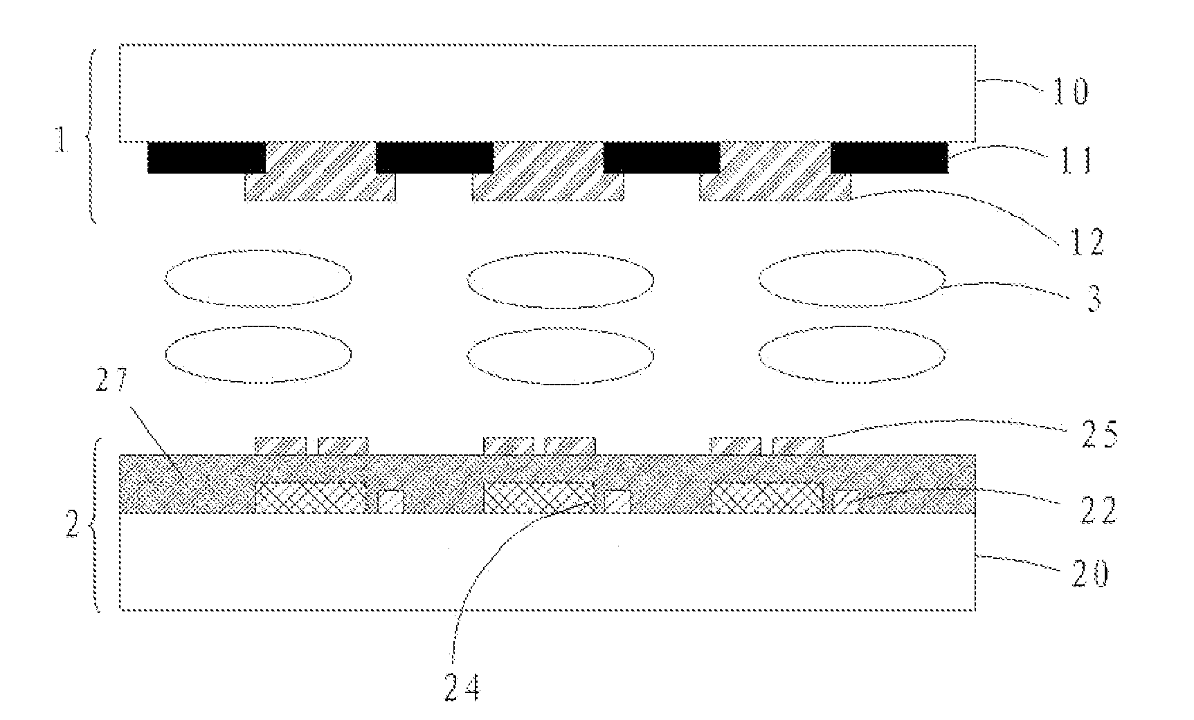
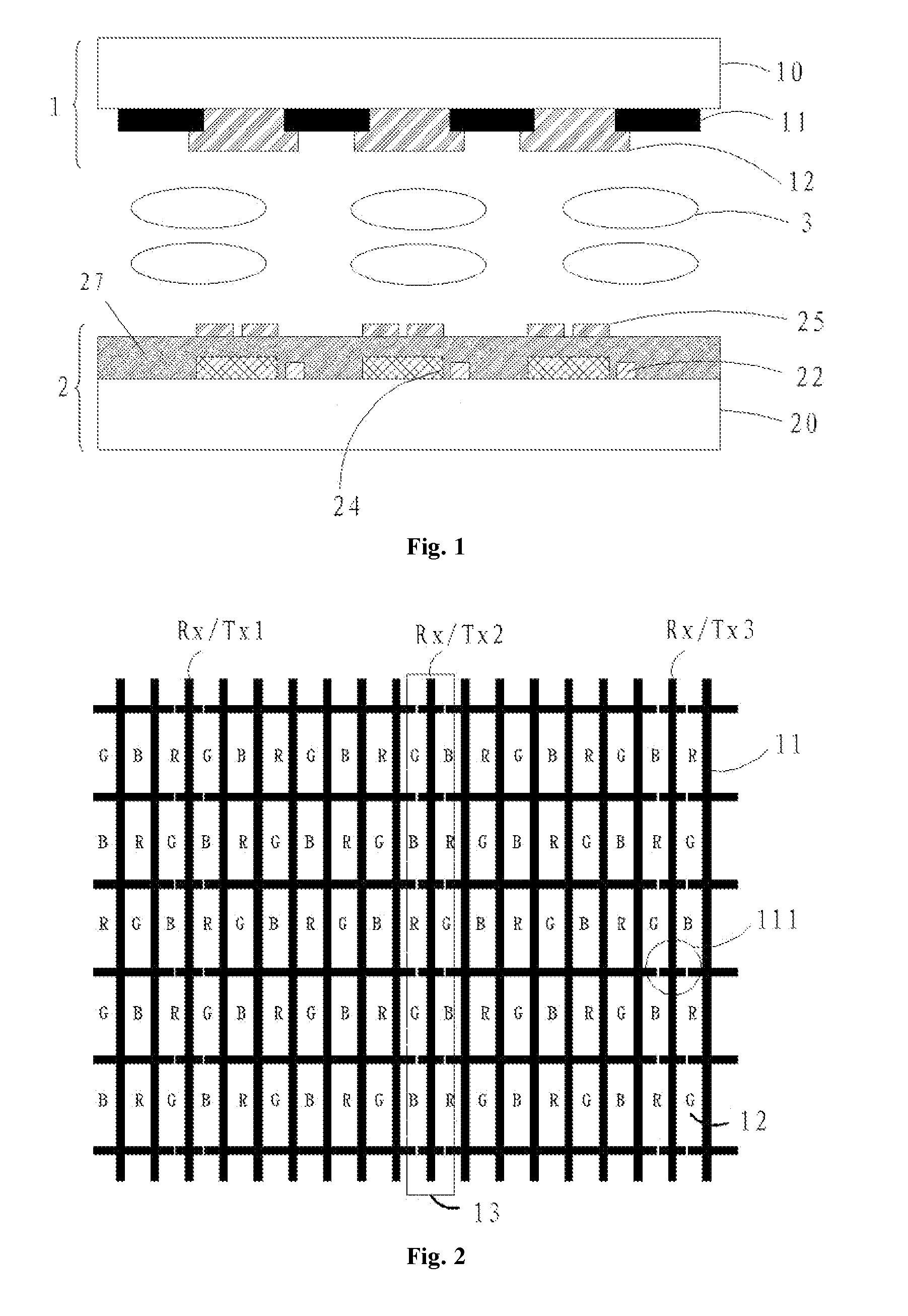
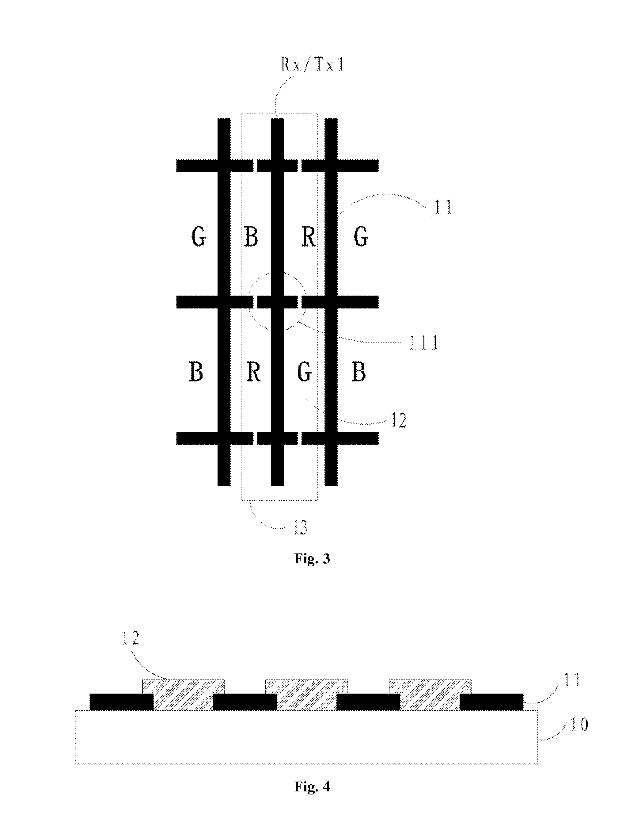
[0032]As shown in FIG. 1, the display panel includes a color film substrate 1 and an array substrate 2 that are aligned with each other to form a cell, and a liquid crystal layer 3 disposed between the color film substrate 1 and the array substrate 2. In general, the array substrate 2 is provided therein with thin film transistors (TFTs) 21 (the thin film transistors 21 are not shown in FIG. 1 and can be seen in FIG. 5) for controlling light emission to implement image display; and the color film substrate 1 is provided therein with a color film layer 12 for achieving image colorization.

[0033]In order to prevent light leak between pixel structures of the display panel to influence display effect, the color film substrate 1 is generally also provided therein with a light blocking layer 11. In general, the light blocking layer 11 is arranged in the color film substrate 1, and the scanning signa...

second embodiment

[0046]The embodiment provides a display panel applicable to an Organic Light-Emitting Diode (OLED) display device.

[0047]An OLED is a light emitting device using an organic solid-state semiconductor as a light emitting material, and there is a most mature technology for white organic light emitting diode (White OLED, namely WOLED), which has a good stability, a simple manufacturing process, and thus is widely applied in display devices. Like a crystal liquid display device, a WOLED display device usually needs a color film layer therein to achieve colorization.

[0048]With progress of display technology, there has emerged such a mode in the WOLED display device that a color film layer is arranged on an array substrate (Color Filter on Array, abbreviated as COA) to achieve a color display mode. In the embodiment, the display panel is formed in the COA mode, the display panel including an array substrate and organic electroluminescent diodes located above the array substrate, the light b...

third embodiment

[0053]The embodiment provides a display device including the display panel in the embodiment or the second embodiment.

[0054]The display device may be a liquid crystal panel, electronic paper, an OLED panel, a mobile phone, a tablet computer, a television, a display, a notebook computer, a digital photo frame, a navigator, or any other product or component with a display function.

[0055]The display device integrates display and touch together, and as the display panel adopted therein has a high transmittance, the display device has good display quality.


PUM

PropertyMeasurementUnit
widthaaaaaaaaaa
widthaaaaaaaaaa
electroconductive propertiesaaaaaaaaaa

Abstract

The present invention relates to the field of display technology, and particularly relates to a display panel, a driving method thereof, and a display device. The display panel comprises a light blocking layer formed of a material with light blocking and electroconductive properties, the light blocking layer including an isolation part electrically isolated from other part of the light blocking layer, the isolation part being further configured to emit a touch driving signal and / or receive a touch sensing signal to achieve a touch control function of the display panel. The display panel has both display function and touch control function, and has a simpler structure and a higher transmittance; the manufacturing process is simpler, and meanwhile, the production cost is reduced and the product yield is improved.

Description

FIELD OF THE INVENTION[0001]The present invention relates to the field of display technology, and particularly relates to a display panel, a driving method thereof, and a display device.BACKGROUND OF THE INVENTION[0002]Touch panels are currently newest information input devices, and can simply, conveniently and naturally implement human-machine interaction and provide a brand new multimedia human-machine interaction method, making people feel visual and tactile enjoyment. With rapid changes of display technology and increasingly fierce competition, it has become a trend to implement a touch display structure with a low cost and high performance.[0003]Display devices with a touch control function can be divided into a resistance type, a capacitance type, a surface acoustic wave type, an infrared type and the like according to the sensing principle, and can be divided into an out-cell structure, an on-cell structure and an in-cell structure according to the structural relation between...

Claims


Application Information

Patent Timeline
Patent Type & Authority Applications(United States)
IPC IPC(8): G06F3/041H01L27/32G02F1/1333G06F3/047G02F1/1335
CPCG06F3/0412G06F3/0416G06F3/047G02F1/133514H01L27/3276G02F1/133512H01L27/323H01L27/3272G02F1/13338G02F2202/16G06F2203/04103G06F3/0445G06F3/0446G06F3/04184H10K59/40H10K59/8792H10K50/865H10K59/126H10K59/131
Inventor XU, ZOUMINGHU, MINGLUO, HONGQIANGGONG, WEIGANG
Owner BOE TECH GRP CO LTD
Learn More