THz RADIATION DETECTION IN STANDARD CMOS TECHNOLOGIES BASED ON THERMIONIC EMISSION

a technology of thermionic emission and thz radiation, applied in the field of thz radiation detection, can solve the problems of low sensitivity, limitations of known detectors, and inability to realize the effect of thz radiation, and achieve the effect of improving increasing the responsivity to thz radiation

Active Publication Date: 2016-10-20
UNIVERSITY OF ROCHESTER
View PDF0 Cites 19 Cited by
  • Summary
  • Abstract
  • Description
  • Claims
  • Application Information

AI Technical Summary

Benefits of technology

[0006]The examples of new THz detectors described in this patent specification unexpectedly demonstrate that in certain structural conditions and under sub-threshold biasing conditions (or weak inversion), semiconductor devices such as MOSFETs can exhibit dramatic increases in responsivity to THz radiation. According to current understanding, it is believed that under sub-threshold biasing conditions and with the correct structure, the plasmonic detection of signals in THz frequency range in a MOSFET becomes negligible compared to the detection from thermionic emission (TE) through a potential barrier between a highly-doped source region and depleted channel, as described below. The detection current due to TE has been found to be a much stronger function of the applied THz signal (exponential dependence) than the detection current due to plasmonic rectification in the channel alone (a square-law dependence), and with properly extended source regions in accordance with some of the embodiments described in more detail below, a MOSFET in a weak inversion can exhibit much improved responsivity to the THz radiation.

Problems solved by technology

Despite such potential advantages of THz radiation, progress in utilizing it has been hindered by difficulties in detecting such radiation.
The known detectors have limitations such as low sensitivity, slow speed, requirements for cryogenic cooling, and difficulty scaling to array formats suitable for THz imaging.
Proposals have been made for using CMOS transistors but in modes that suffer from low efficiency particularly at higher frequencies.
Infrared focal plane arrays (FPAs) have been proposed for THz imaging experiments but the detection efficiency is believed low, typically less than 5%.
The challenge of discovering efficient and effective THz detectors has remained for a long time.

Method used


Image

  • THz RADIATION DETECTION IN STANDARD CMOS TECHNOLOGIES BASED ON THERMIONIC EMISSION
  • THz RADIATION DETECTION IN STANDARD CMOS TECHNOLOGIES BASED ON THERMIONIC EMISSION
  • THz RADIATION DETECTION IN STANDARD CMOS TECHNOLOGIES BASED ON THERMIONIC EMISSION

Examples


Embodiment Construction

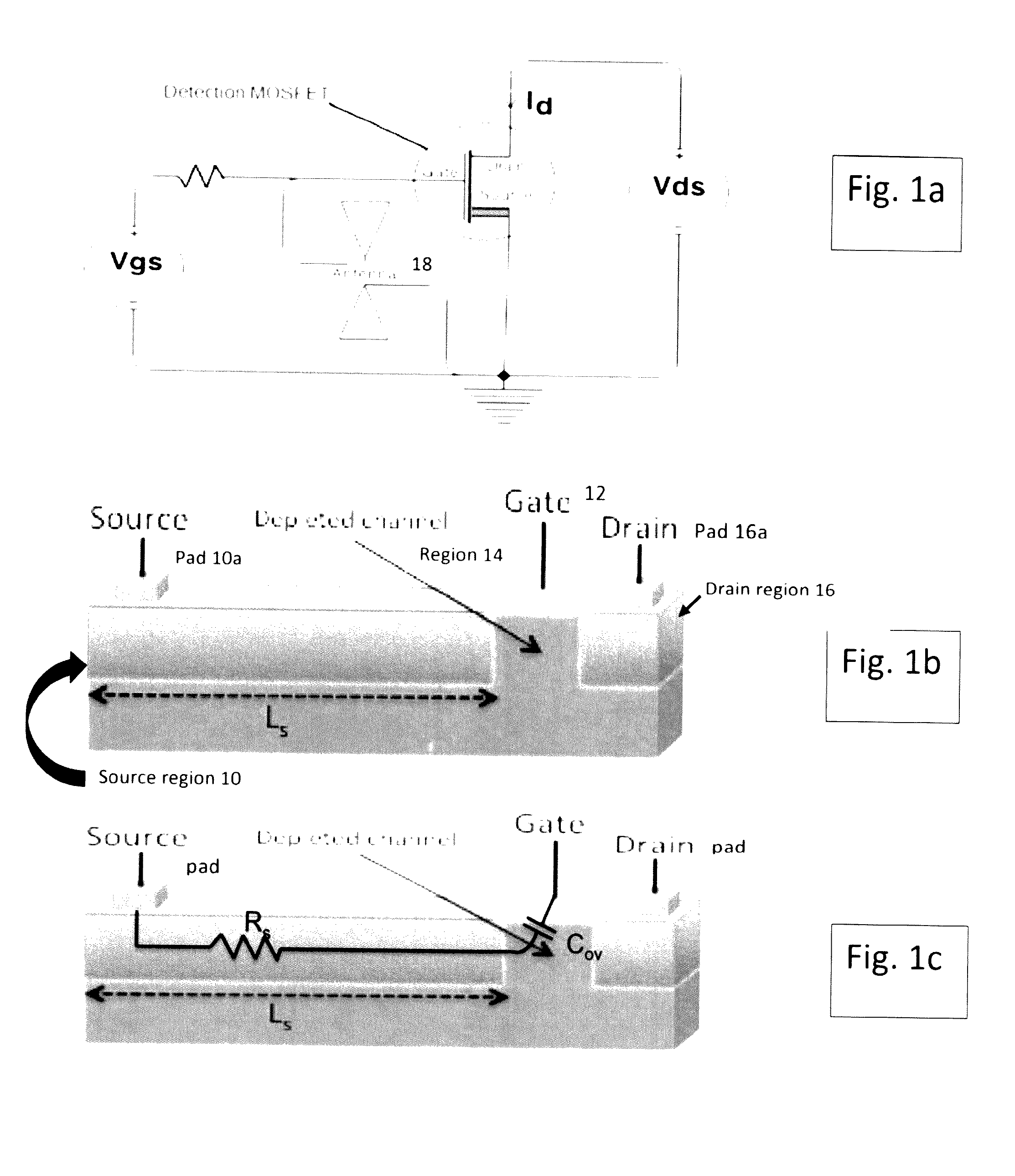
[0022]FIG. 1a illustrates a simplified schematic of a pixel for detecting THz energy that can be referred to as a THz signal. In accordance with some of the disclosed embodiments, the device in this example comprises a MOSFET (metal oxide semiconductor field effect transistor) implemented as an NMOS transistor that has an otherwise typical or standard structure but notably has an extended source region 10 that has a length Ls as illustrated in FIG. 1b, which has a significantly greater dimension than in a standard MOSFET. The biasing voltage Vgs between gate 12 and source pad 10a is kept below the threshold voltage Vt or Vth of the transistor so that the channel region 14 is depleted of free carriers and forms a depleted channel acting as a potential barrier at the source-channel boundary (i.e., the height of the potential barrier is set by the biasing voltage Vgs). The drain-source voltage Vds between drain region 16 and source region 10 is maintained high enough so that the drain ...


PUM


Abstract

A detector of terahertz (THz) energy includes a MOSFET having an extended source region, and a channel region depleted of free carriers, which MOSFET operates in a sub-threshold voltage state and has an output that is an exponential function of THz energy supplied to the gate.

Description

FIELD[0001]This patent specification pertains to detection of teraherz (THz) radiation and more specifically to detecting THz energy using an operating regime of semiconductor devices such as CMOS transistors that conventionally is called the OFF (non-conducting) state, and to utilizing such detection in imaging, communications, and other fields.BACKGROUND[0002]Several references, cited at the end of this patent specification, are identified by numbers in square brackets in the description below and are hereby incorporated by reference.[0003]THz radiation typically denotes electromagnetic energy in an ITU-designated band of frequencies from 0.3 to 3 terahertz (1 THz=1012 Hz) and wavelengths ranging from 1 mm to 0.1 mm (100 μm). This is a range between microwaves and infrared light, and shares some properties with each. Like infrared and microwave radiation, THz radiation is understood to travel in a line-of-sight and to be non-ionizing, which makes it safer for biological tissue. Li...

Claims


Application Information

Patent Timeline
Patent Type & Authority Applications(United States)
IPC IPC(8): G01J5/08G01J5/22H01L31/112
CPCG01J5/0837H01L31/112G01J5/20G01J2005/106G01J5/00G01J5/22G01J1/42G01J3/42H01L31/1136
Inventor IGNJATOVIC, ZELJKODERY, HANAN
Owner UNIVERSITY OF ROCHESTER
Why Eureka
Try Eureka