Semiconductor light emitting device

a light-emitting device and semiconductor technology, applied in the direction of semiconductor devices, basic electric elements, electrical equipment, etc., can solve the problems of reducing the carrier injection efficiency of the semiconductor light-emitting device, poor light-emitting efficiency, and difficult to inject holes into the active layer, so as to facilitate the reduction of energy barriers, enhance the effect of hole injection efficiency, and reduce electron leakage curren

Active Publication Date: 2016-11-03
NAT CHIAO TUNG UNIV
View PDF8 Cites 6 Cited by
  • Summary
  • Abstract
  • Description
  • Claims
  • Application Information

AI Technical Summary

Benefits of technology

[0006]The improved electron-blocking layer according to the present invention is a super lattice multi-layer structure constructed by a first layer of quaternary material AlInGaN alternately stacked with a second layer of AlGaN material. The improved electron-blocking layer can not only change the bandgap of the electron-blocking layer to effectively...

Problems solved by technology

However, although the electron-blocking layer containing aluminum may reduce the electron leakage current, which also influence the injection of holes into an active layer.
For example, the electron-blocking layer containing aluminum may form an energy barrier at the valence band, such that it is more difficult to inject the holes into the active layer.
This may reduce the carrier injec...

Method used


Image

  • Semiconductor light emitting device
  • Semiconductor light emitting device
  • Semiconductor light emitting device

Examples


Embodiment Construction

[0019]In the following, specific embodiments are provided to illustrate the detailed description of the present invention. Those skilled in the art can easily conceive the other advantages and effects of the present invention, based on the disclosure of the specification. The present invention can also be carried out or applied by other different embodiments.

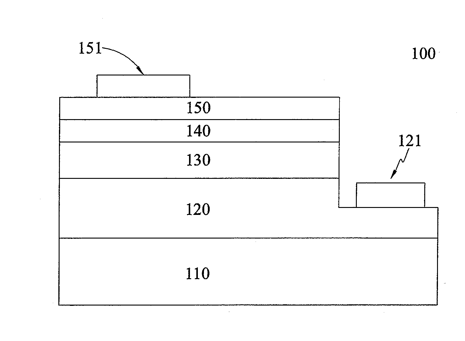
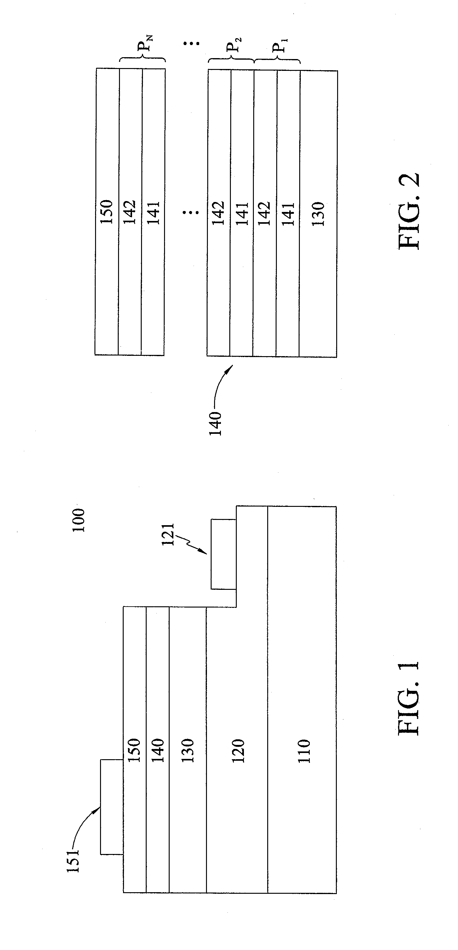
[0020]FIG. 1 is a scheme view of a semiconductor light emitting device 100 having an electron-blocking layer 140 according to an embodiment of the present invention. The light emitting device 100 includes a substrate 110, an N type semiconductor layer 120 formed on the substrate 110, an active layer 130, an electron-blocking layer 140, and a P type semiconductor layer 150 formed on the electron-blocking layer 140.

[0021]As shown in FIG. 1, an N side electrode 121 is formed on a first portion of the N type semiconductor layer 120, and the active layer 130 is formed on a second portion of the N type semiconductor layer 120. The ele...


PUM


Abstract

A light emitting device is provided. The light emitting device includes a substrate, an N type semiconductor layer formed on the substrate, an active layer, an electron-blocking layer, and a P type semiconductor layer formed on the electron-blocking layer. An N side electrode is formed on a first portion of the N type semiconductor layer, and the active layer is formed on a second portion of the N type semiconductor layer. The electron-blocking layer is a super lattice multi-layer structure formed on the active layer, the P type semiconductor layer is formed on the electron-blocking layer, and a P side electrode is formed on a portion of the P type semiconductor layer.

Description

FIELD OF THE INVENTION[0001]The invention relates to a semiconductor light emitting device, and, more particularly, to a semiconductor light emitting device with improved electron-blocking layer.DESCRIPTION OF RELATED ART[0002]In the structure of conventional wide-bandgap semiconductor light emitting device (especially for those with group III-V nitrides), aluminum-containing materials are usually interposed in an electron-blocking layer to effectively reduce electron leakage current. However, although the electron-blocking layer containing aluminum may reduce the electron leakage current, which also influence the injection of holes into an active layer. For example, the electron-blocking layer containing aluminum may form an energy barrier at the valence band, such that it is more difficult to inject the holes into the active layer. This may reduce the carrier injection efficiency of the semiconductor light emitting device, and lead an issue of poor light emitting efficiency.[0003]...

Claims


Application Information

Patent Timeline
IPC IPC(8): H01L33/06H01L33/32H01L33/00H01L33/14
CPCH01L33/06H01L33/0025H01L33/32H01L33/145H01L33/04
Inventor CHANG, CHUN-YENLI, ZHEN-YUKUO, HAO-CHUNG
Owner NAT CHIAO TUNG UNIV
Why Eureka
Try Eureka