

Exposure apparatus, resist pattern forming method, and storage medium
a technology of resist pattern and exposure apparatus, which is applied in the direction of microlithography exposure apparatus, photomechanical treatment, instruments, etc., can solve the problems of low throughput (number of substrates processed per unit time), affecting the uniformity of the in-plane image, and difficulty in appreciating the light intensity. , to achieve the effect of facilitating the adjustment of the exposure amount and high uniformity
- Summary
- Abstract
- Description
- Claims
- Application Information
AI Technical Summary
Benefits of technology
Problems solved by technology
Method used
Image

Examples
first embodiment
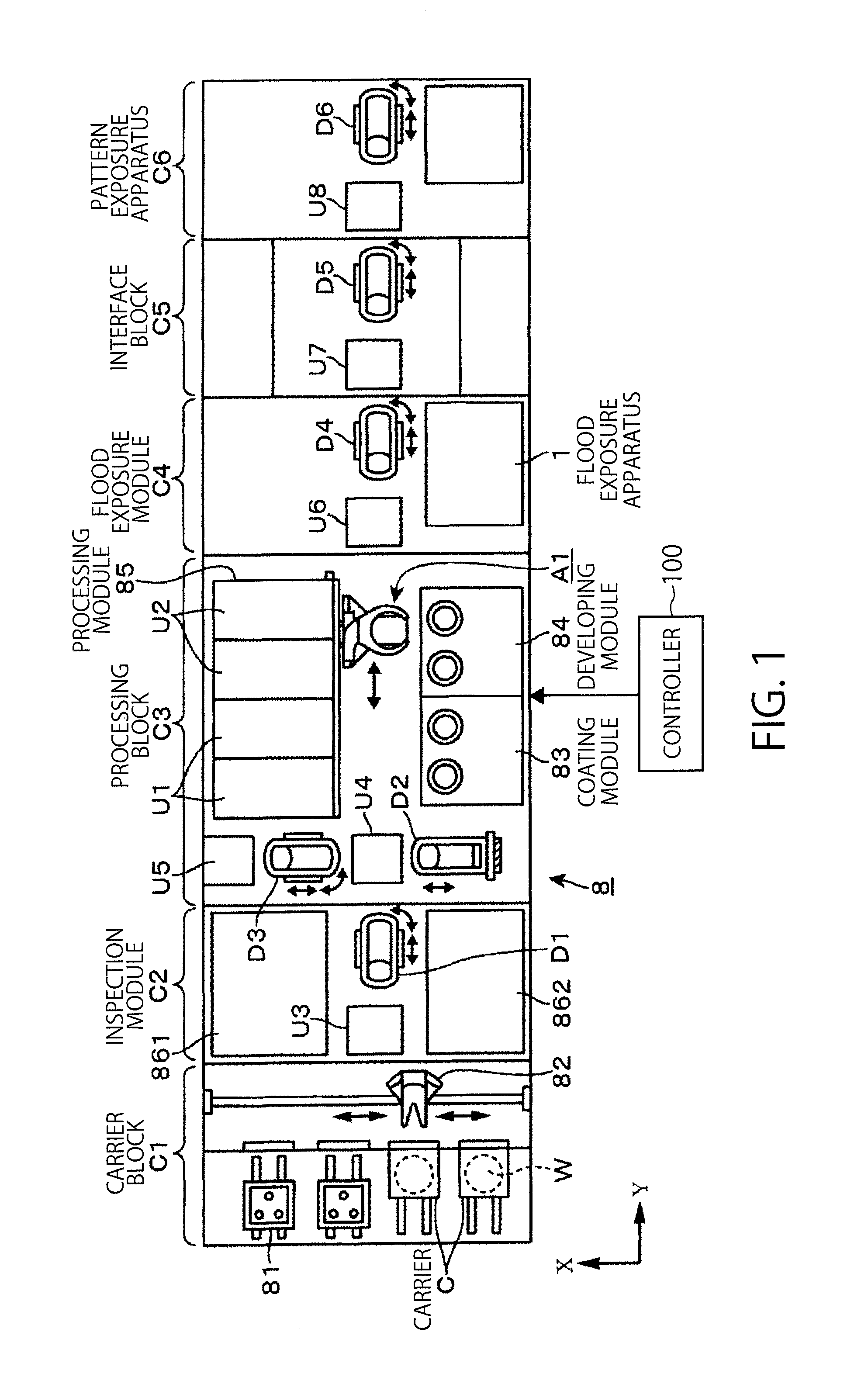
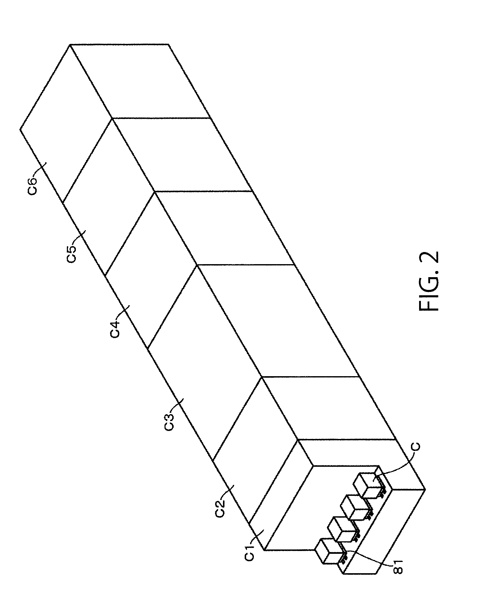
[0038]The construction of a coating / developing apparatus 8 including an exposure apparatus according to an embodiment of the present invention will now be described with reference to FIGS. 1 and 2. FIG. 1 is a plan view of a system including the coating / developing apparatus 8 and a pattern exposure apparatus C6 connected to the apparatus 8; and FIG. 2 is a perspective view of the system. The coating / developing apparatus 8 is provided with a carrier block C1. A wafer W, housed in a sealed carrier C placed on a stage 81, is taken out by a transfer arm 82. The transfer arm 82 functions to transfer a wafer W after development to an inspection module C2, and to receive a wafer W after inspection from the inspection module C2 and return the wafer W to the carrier C. The inspection module C2 is a module to inspect the line width of a pattern formed on a processed wafer W, as described below.
[0039]A wafer W, which has been transported to the inspection module C2, is once placed on a transfe...
second embodiment
[0079]A flood exposure apparatus 1 according to a second embodiment will now be described with reference to FIGS. 9 and 10. In the following description, the same reference numerals as used for the first embodiment are used to refer to the same components, and a detailed description thereof is omitted.
[0080]First, a wafer W on which a pattern has been formed in the pattern exposure apparatus C6 is transported into the flood exposure apparatus 1. Subsequently, a strip-shaped irradiation area L1, having a length which is equal to or a slightly longer than the diameter of the wafer W, is formed by means of the exposure section 11 in the same manner as in the first embodiment. While allowing the irradiation area L1 to lie along the diameter of the wafer W, a rotating mechanism 15 connected to the stage 13 supporting the wafer W is rotated to rotate the wafer W through, for example, 180 degrees or the integral multiple of 180 degrees, thereby allowing the irradiation area L1 to scan the ...
third embodiment
[0092]In the first embodiment and the second embodiment, while exposing a wafer W with the strip-shaped irradiation area L1, the irradiation area L1 is continuously moved relative to the wafer W. In the third embodiment, on the other hand, flood exposure is performed in a stepwise manner like pattern exposure performed in the pattern exposure apparatus C6.
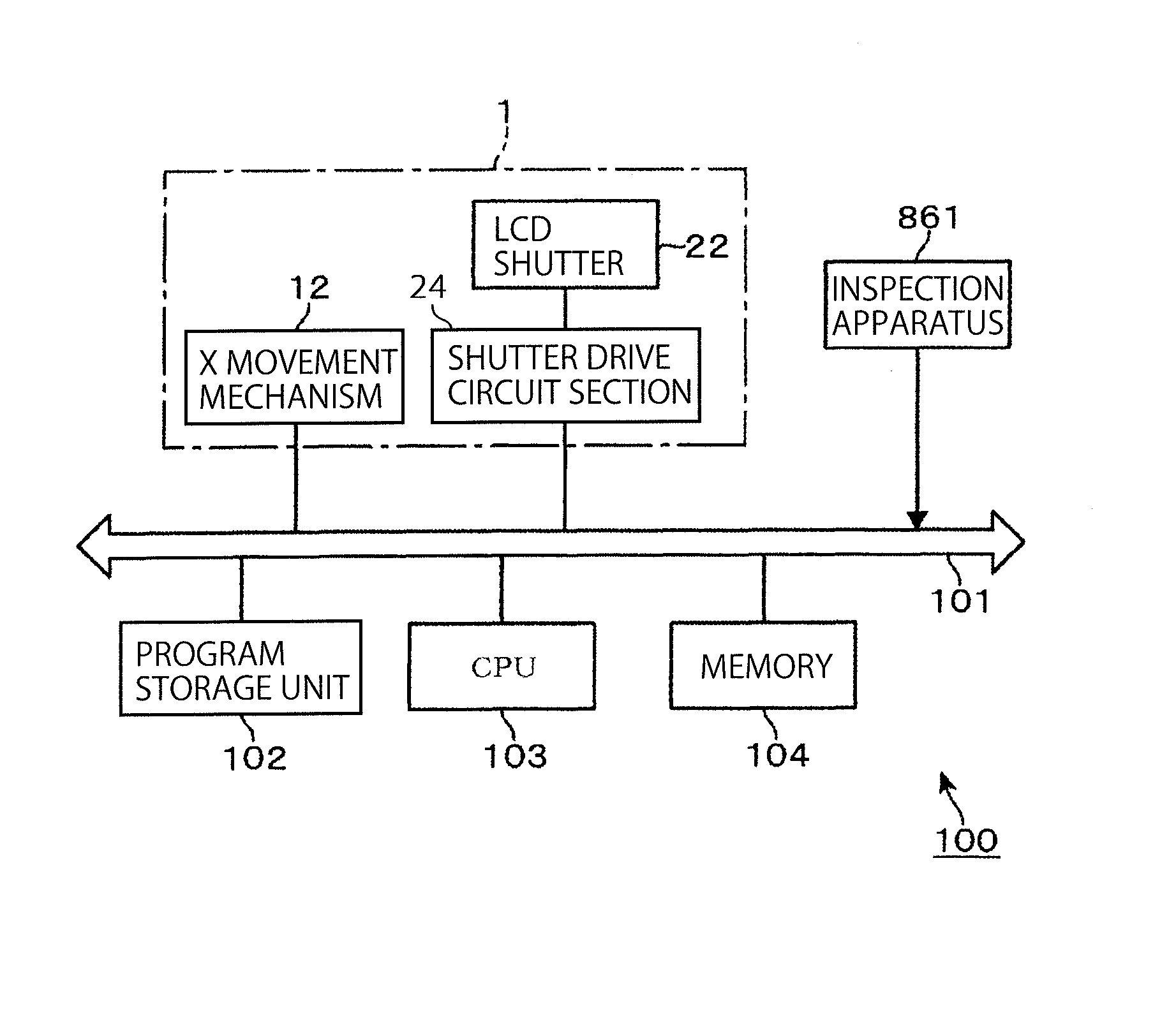
[0093]In particular, as shown in FIG. 12, in the flood exposure apparatus 1 according to the third embodiment, the stage 13 is configured to be movable both in the X-direction and in the Y-direction by means of the X movement mechanism 12 and a Y movement mechanism 16. Further, the coating / developing apparatus 8 includes a controller 100 as shown in FIG. 14.
[0094]In flood exposure according to this embodiment, a light irradiation area is formed as an area corresponding to an exposure shot area formed during pattern exposure performed in the pattern exposure apparatus C6. In pattern exposure performed in the pattern exposure apparat...
PUM
 Abstract
Description
Claims
Application Information