Micromechanical pressure sensor device and corresponding manufacturing method
- Summary
- Abstract
- Description
- Claims
- Application Information
AI Technical Summary
Benefits of technology
Problems solved by technology
Method used
Image

Examples
Embodiment Construction
[0028]Identical or functionally equivalent elements are denoted by the same reference numerals in the figures.
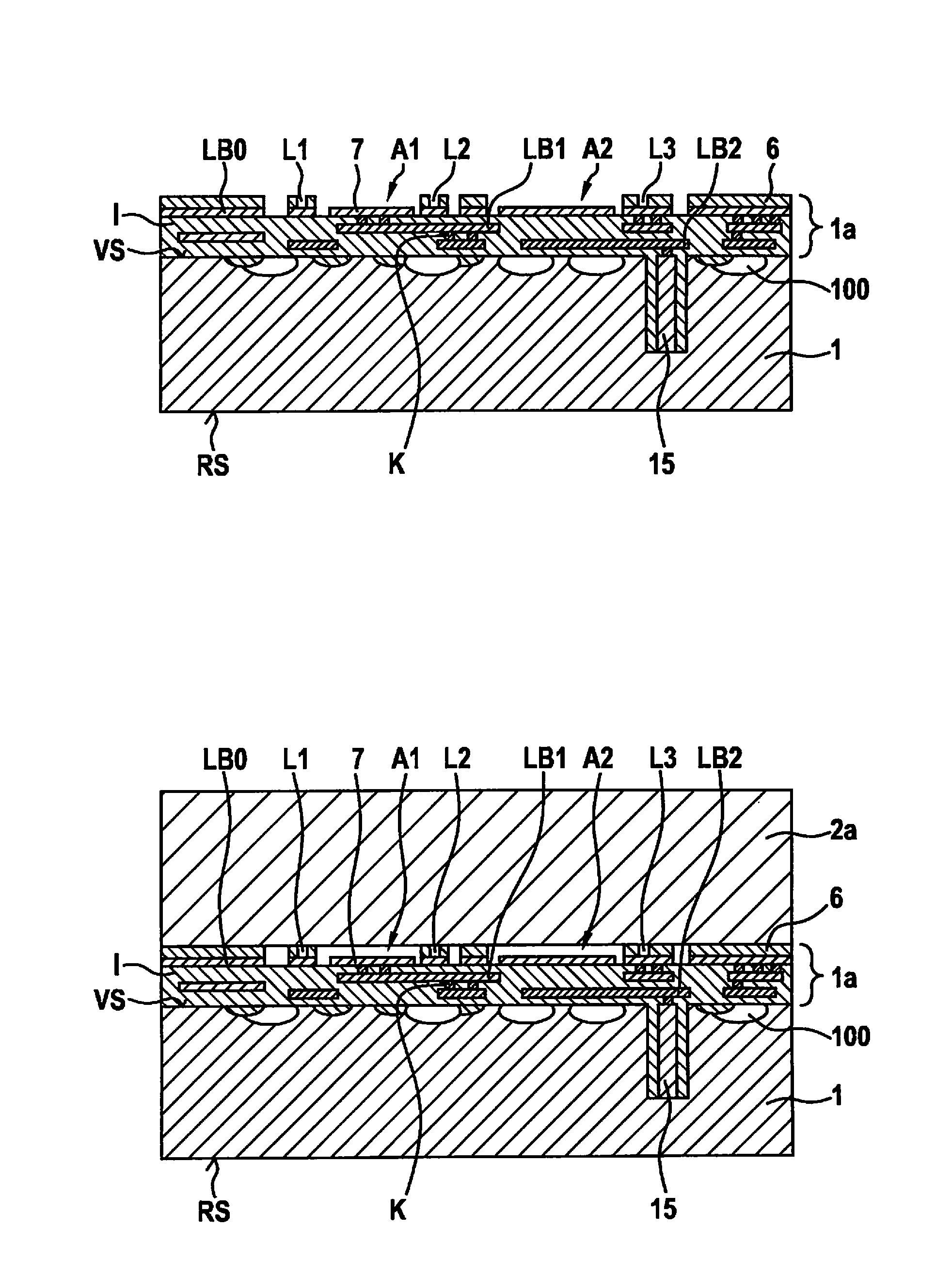
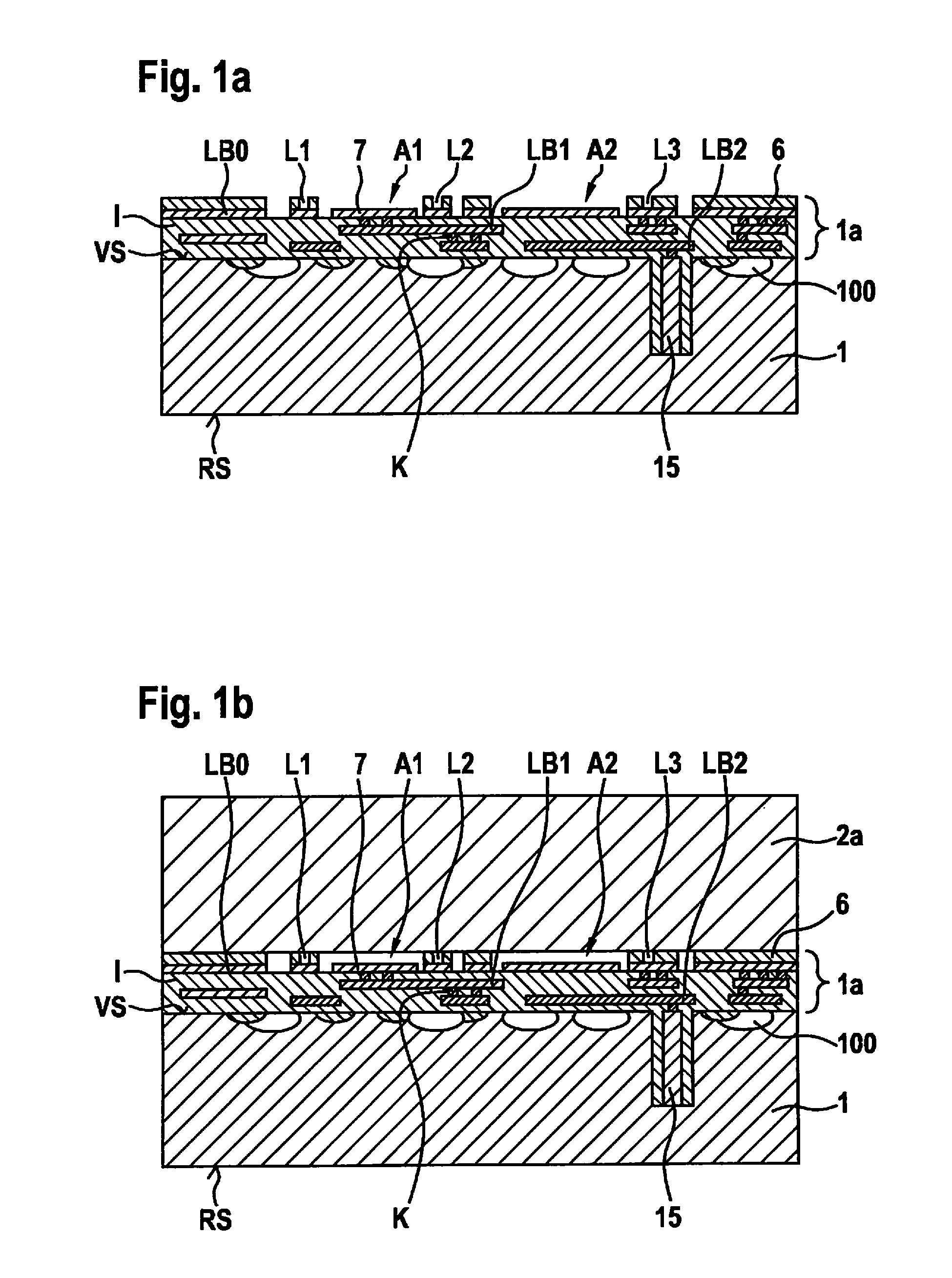
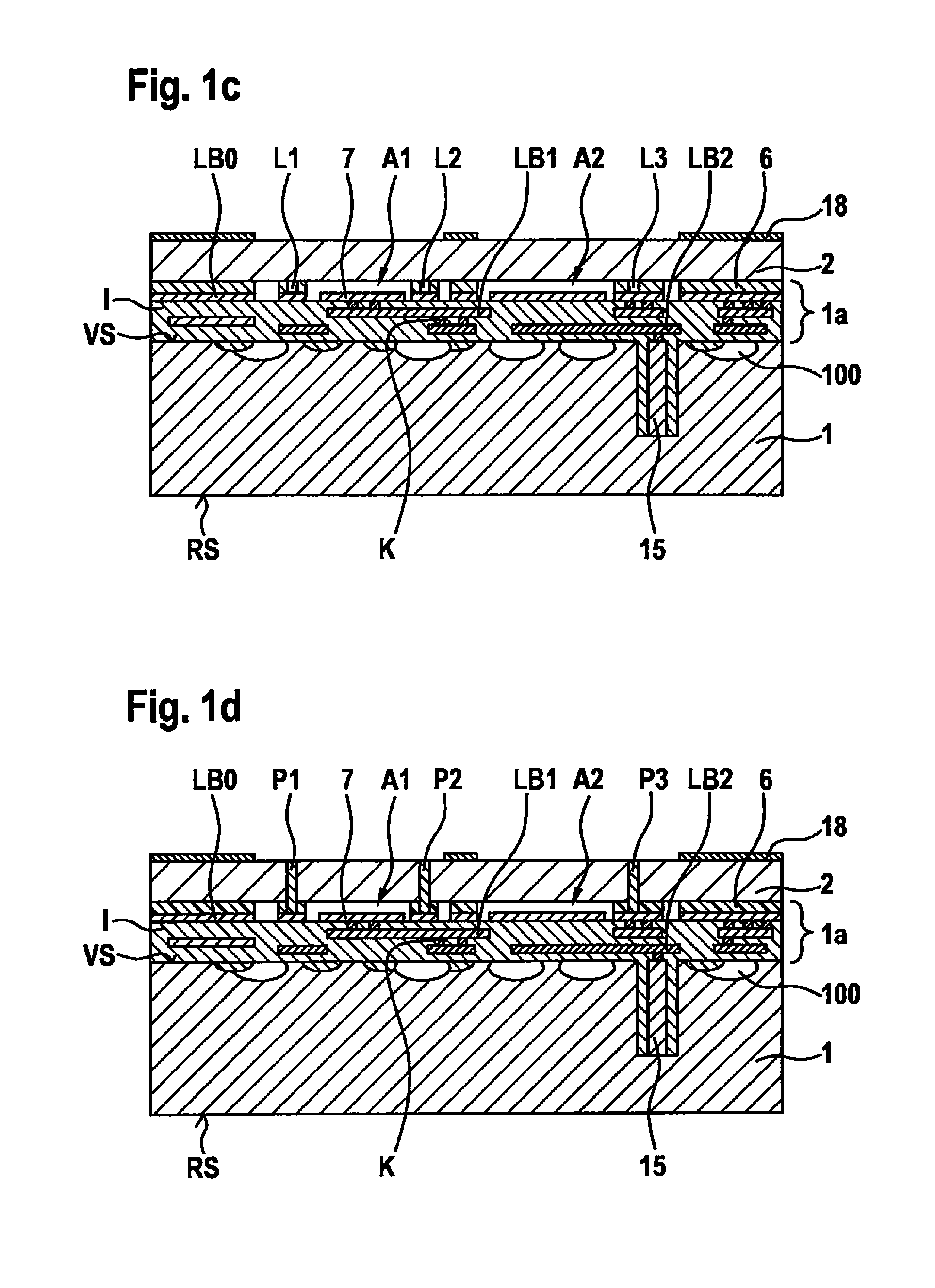
[0029]FIGS. 1a) through 1h) show schematic cross-sectional views for explaining a micromechanical pressure sensor device and a corresponding manufacturing method according to a first specific embodiment of the present invention.
[0030]In FIG. 1a), reference numeral 1 denotes a CMOS wafer which includes a plurality of CMOS circuits 100 which include, for example, an evaluation circuit for the micromechanical pressure sensor device to be formed.
[0031]The CMOS wafer has a front side VS and a rear side RS. On front side VS of CMOS wafer 1, a rewiring system 1a is formed which includes a plurality of strip conductor levels LB0, LB1, LB2 and insulating layers I situated in between. To simplify the illustration, insulating layers I in which strip conductor levels LB0, LB1, LB2 are embedded are not separately illustrated. The strip conductor sections of strip conductor levels LB0, LB...
PUM
| Property | Measurement | Unit |
|---|---|---|
| Temperature | aaaaa | aaaaa |
| Time | aaaaa | aaaaa |
| Pressure | aaaaa | aaaaa |
Abstract
Description
Claims
Application Information
 - R&D
- Intellectual Property
- Life Sciences
- Materials
- Tech Scout
- Unparalleled Data Quality
- Higher Quality Content
- 60% Fewer Hallucinations
Browse by: Latest US Patents, China's latest patents, Technical Efficacy Thesaurus, Application Domain, Technology Topic, Popular Technical Reports.
© 2025 PatSnap. All rights reserved.Legal|Privacy policy|Modern Slavery Act Transparency Statement|Sitemap|About US| Contact US: help@patsnap.com