Image sensor, optoelectronic system comprising said image sensor, and method for manufacturing said image sensor

an optoelectronic system and image sensor technology, applied in the field of image sensors, can solve the problems of reducing the effective frame rate of the image sensor, blurring effects, and increasing the design requirements of the readout circuit, and achieve the effect of increasing the response of the photosensitive element as described in the claims, and enhancing the respons

Active Publication Date: 2016-12-15
FUNDACIO INST DE CIENCIES FOT NIQUES
View PDF0 Cites 12 Cited by
  • Summary
  • Abstract
  • Description
  • Claims
  • Application Information

AI Technical Summary

Problems solved by technology

On the other hand, increasing the exposure time reduces the effective frame rate of the image sensor and may lead to blurring effects.
Moreover, a longer exposure time enhances the adverse effect of thermal noise, which in turn makes the design requirements for the readout circuit even more demanding.
Other known technologies, such as for instance avalanche photodiodes or image intensifiers, despite being able to provide photodetectors with some photoconductive gain via carrier multiplication effects, have proven to be difficult to integrate into high-resolution image sensors.
Moreover, these technologies require operation conditions that are unsuitable for practical image sensors (e.g. avalanche photodiodes typically require very high reverse bias voltages for proper operation), as described for example in chapter 2 of “Smart CMOS Image Sensors and Applications”, Jun Ohta, CRC Press, Sep. 19 2007.
However, such image sensors typically exhibit limited photoconductive gain.
However, the device can only achieve desired responsivity levels at the expense of increased dark current levels, which in turn degrade the sensitivity and the shot-noise limit of the device.
This means that a monolithic integration of the plurality of pixels of an image sensor with the readout circuit of said pixels can only be achieved for those image sensors designed to operate in the visible and / or near infrared ranges.
Such hybrid integration involves difficult and costly bonding processes, as described for example in US 2008 / 093554 A1 and in U.S. Pat. No. 6,107,618 A, which in turn impose a lower limit on the pixel size.

Method used


Image

  • Image sensor, optoelectronic system comprising said image sensor, and method for manufacturing said image sensor
  • Image sensor, optoelectronic system comprising said image sensor, and method for manufacturing said image sensor
  • Image sensor, optoelectronic system comprising said image sensor, and method for manufacturing said image sensor

Examples


Embodiment Construction

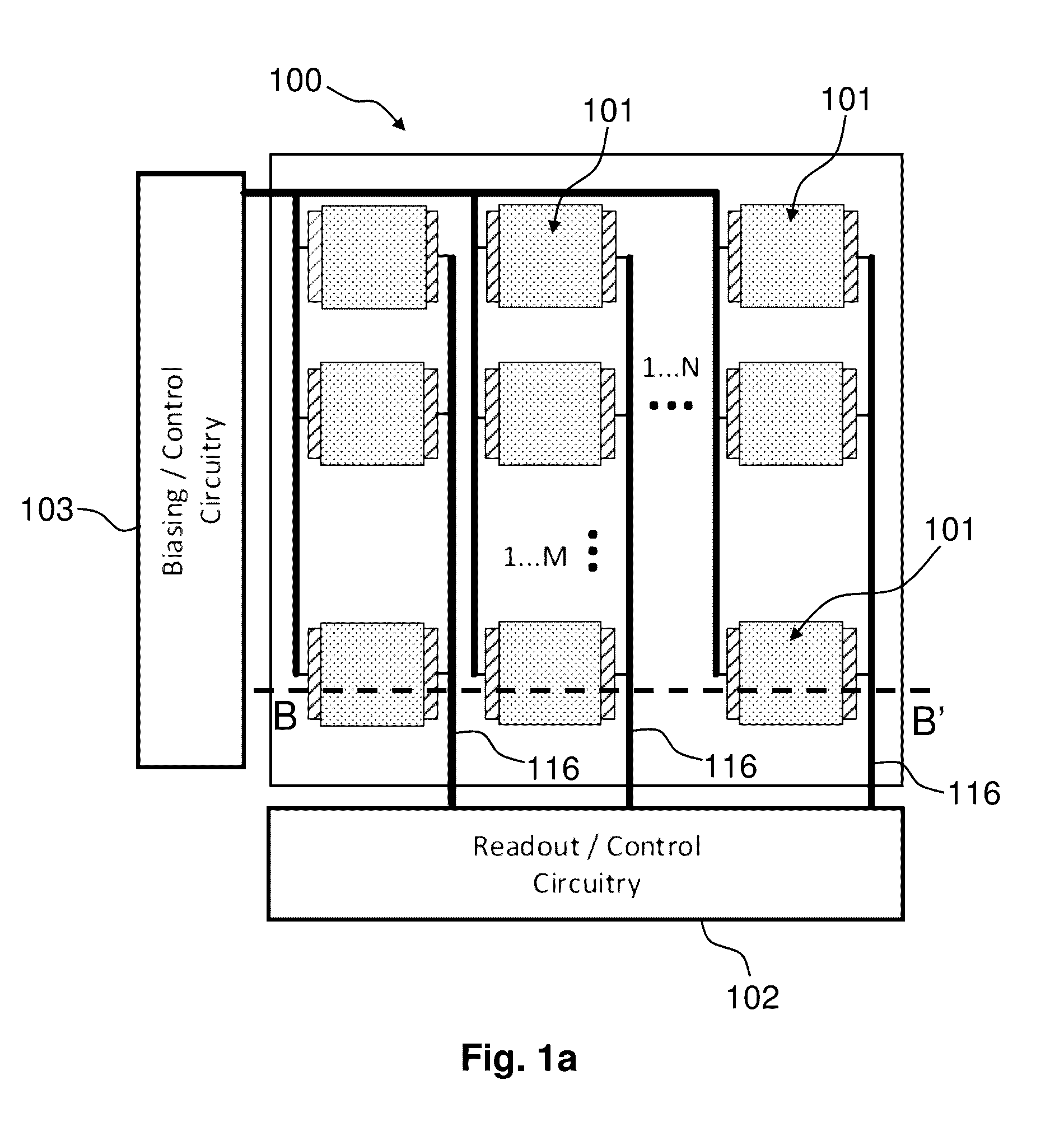
[0194]In FIG. 1a it is illustrated a top plan view of a block diagram of an embodiment of the image sensor according to present invention. In particular the image sensor 100 comprises a plurality of pixels 101 arranged as a two-dimensional array of M rows and N columns. The plurality of pixels 101 are operatively connected to a control unit that includes a biasing circuit 103 for biasing the plurality of pixels 101 and a readout circuit 102 for selectively reading out the photo-signals generated by the light impinging on the plurality of pixels 101.

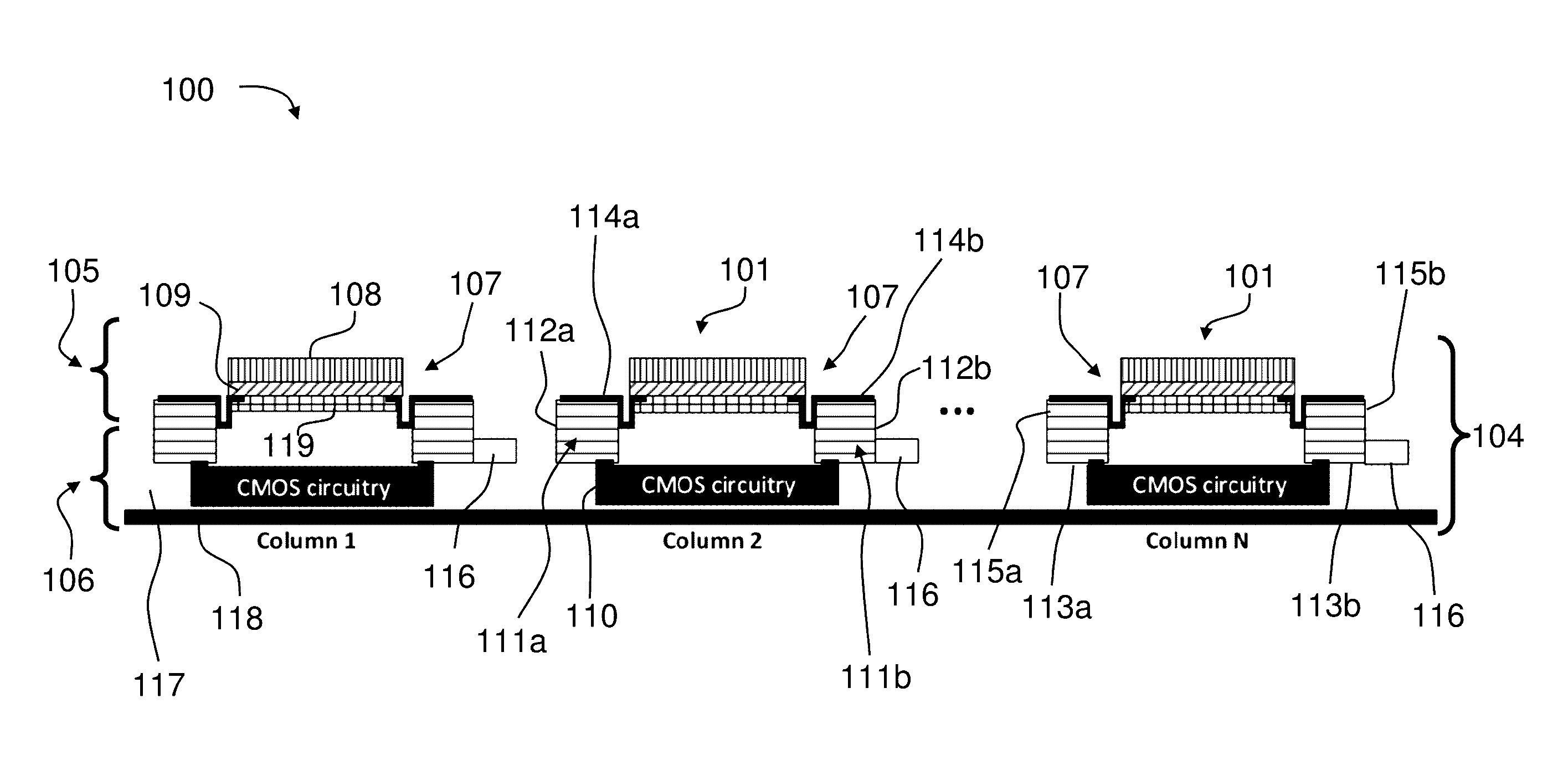
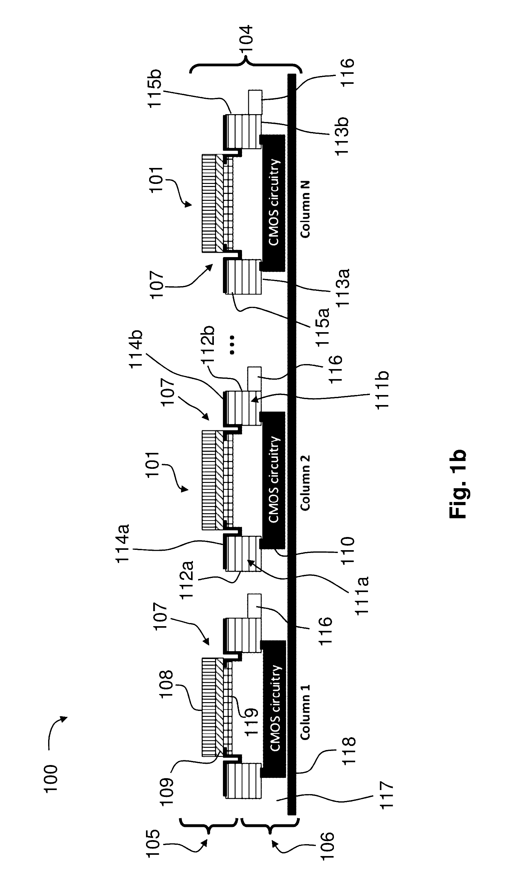
[0195]As it can be better seen in the cross-sectional view of FIG. 1b, the image sensor 100 comprises a monolithic three-dimensional integrated circuit 104 comprising an upper level 105 having a first plurality of stacked layers and a lower level 106, disposed underneath the upper level, having a second plurality of stacked layers.

[0196]Each pixel 101 of the plurality of pixels comprises a photosensitive element 107 arranged at a selected...


PUM


Abstract

The invention relates to an image sensor comprising a plurality of pixels operatively connected to a control unit that includes a readout circuit, characterized in that it comprises a monolithic three-dimensional integrated circuit comprising an upper level and a lower level; wherein each pixel comprises: a photosensitive element arranged in said upper level and comprising a photosensitizing layer associated to a transport layer; an active device arranged in said lower level and operatively coupled to the photosensitive element; and a first intermediate terminal and an output terminal circuitally connected, respectively, to the photosensitive element and to the readout circuit; wherein the image sensor further comprises a dark current suppressing circuit; and wherein the control unit is configured to, upon readout of a pixel, circuitally connect the first intermediate terminal of said pixel with its output terminal through the dark current suppressing circuit. The invention also relates to an optoelectronic system comprising said image sensor and to a method of manufacturing said image sensor.

Description

CROSS REFERENCE TO RELATED APPLICATION[0001]This application is based on and claims priority to European Patent Application Serial No. 15171314.6, filed Jun. 10, 2015, the disclosure of which is incorporated by reference herein in its entirety.FIELD OF THE INVENTION[0002]The present invention relates to the field of image sensors, in particular image sensors comprising a plurality of pixels operatively connected to a control unit that includes a readout circuit for selectively reading out the plurality of pixels. An image sensor according to the present invention achieves a simple and efficient integration of the plurality of pixels with the control unit in a small footprint, leading to a compact integrated circuit architecture, and attains an improved pixel sensitivity. Moreover, the particular pixel design of the image sensor of the invention makes it possible to obtain pixels with high photoconductive gain, enhanced responsivity, and / or short response time. The present invention ...

Claims


Application Information

Patent Timeline
Patent Type & Authority Applications(United States)
IPC IPC(8): H04N5/361H04N5/374H04N5/378H01L27/146
CPCH04N5/361H01L27/14689H01L27/14643H04N5/378H01L27/14636H04N5/374H01L27/14612H01L27/146H01L27/14605H01L27/14683H01L27/14623H01L27/14632H01L27/14634H01L27/14645H01L27/14603H04N25/63H04N25/75H04N25/76
Inventor KONSTANTATOS, GERASIMOSKOPPENS, FRANKGOOSSENS, STIJNPIQUERAS, JUAN JOSEPEREZ, RA L
Owner FUNDACIO INST DE CIENCIES FOT NIQUES
Why Eureka
Try Eureka