Method of manufacturing a plurality of island-shaped dipoles having self-aligned electrodes

a technology of self-alignment and dipoles, which is applied in the direction of diodes, electric devices, solid-state devices, etc., can solve the problems of increasing difficulty, increasing the number of components per surface area, and affecting the accuracy of manufacturing methods, so as to achieve the effect of easy connection of dipoles

Active Publication Date: 2016-12-29
COMMISSARIAT A LENERGIE ATOMIQUE ET AUX ENERGIES ALTERNATIVES
View PDF2 Cites 6 Cited by
  • Summary
  • Abstract
  • Description
  • Claims
  • Application Information

AI Technical Summary

Benefits of technology

[0012]The present disclosure aims at providing a method of manufacturing an array of island dipoles each requiring two connections to different respective levels, enabling to easily connect the dipoles, including for array pitches considered small as compared with the accuracy of manufacturing techniques.
[0021]In other words, the isotropic character of the etching, which thus etches the layer of material in all directions, causes an overetching under the solid patterns. The islands are thus manufactured by means of a single etch step, while however being topped with protective “umbrellas”. Such umbrellas naturally limit risks of subsequent short-circuits on deposition of the metallizations, so that it is no longer necessary to take subsequent specific measures for this purpose, including when an array of very small pitch is manufactured. For example, it is no longer necessary to provide a passivation layer. A considerable simplification of the manufacturing of dipoles and of their connections is thus obtained. Further, the metallization forming the lower-level connections is directly deposited on the base. Not only is the method further simplified, but also is an electrode naturally obtained in the form of a grid which surrounds the islands. This thus enables to provide a single contacting area for all the connections of the dipoles provided on a lower level, for example, the cathodes of photodiodes, at the periphery of the photodiode. The connection between two levels is thus easy and may be formed simply by providing a connection range of desired height. It can thus be noted that the method allows a self-alignment of the electrodes on manufacturing.
[0022]According to the described embodiments, the etching of the islands comprises, prior to the application of the isotropic etching, a phase during which an anisotropic etching is applied. In other words, the alternation of an anisotropic phase with an isotropic phase enables to adjust the volume of the islands, and thus to adjust the volume of active material of the dipoles.
[0025]According to an embodiment, the islands are gathered in a predetermined area of the base, and the deposition of the electrically conductive material to form the first and second electrodes comprises depositing a layer of said conductive material all over the support (that is, the surface defined by the islands and the base), and thus said area. As previously described, the full plate deposition greatly simplifies the method and enables to simply form an electrode in the form of a grid.
[0027]For very fine pitches, it is advantageous to have the two types of connections (electrodes at the top of the islands and common gates at the bottom of the trenches) at the same level, that is, that defined by the electrodes at the top of the islands. Preferably, the connection located at the bottom of the islands is thus “raised” to the level of the electrodes arranged at the top of the islands.

Problems solved by technology

. . ), that is, the number of components per surface area unit, in electronic circuits often comes up against the limited accuracy of manufacturing methods, particularly photolithography.
Further, the difficulty is all the greater when a plurality of connection levels are present in an electronic component, as is especially the case in an “island”-type dipole, for example, a photodiode (commonly called “mesa” photodiode), which requires applying a potential difference between the top and the foot of the island in order to operate.
This technique is however crippling for arrays of photodiodes of large dimensions due to the series electric resistance implied by said layer.
This structure is however highly area-consuming and the pitch of the array of photodiodes is substantially doubled, which thus limits the photodiode integration density.
Further, when the cathode contacting area is formed directly at the bottom of trench 36, the access thereto becomes very difficult if the trench diameter is small.
This thus requires at best very accurate alignment tools, which are thus very expensive.
At worst, it is impossible to go below a given array pitch.
However, a problem is then posed in the forming of opening 46 providing access to the N layer for the cathode design.

Method used


Image

  • Method of manufacturing a plurality of island-shaped dipoles having self-aligned electrodes
  • Method of manufacturing a plurality of island-shaped dipoles having self-aligned electrodes
  • Method of manufacturing a plurality of island-shaped dipoles having self-aligned electrodes

Examples


Embodiment Construction

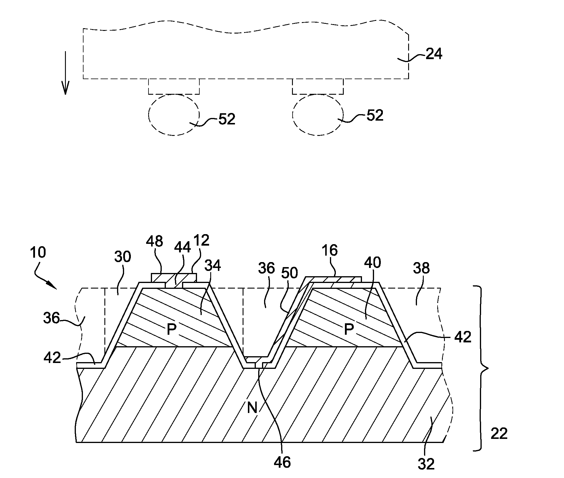
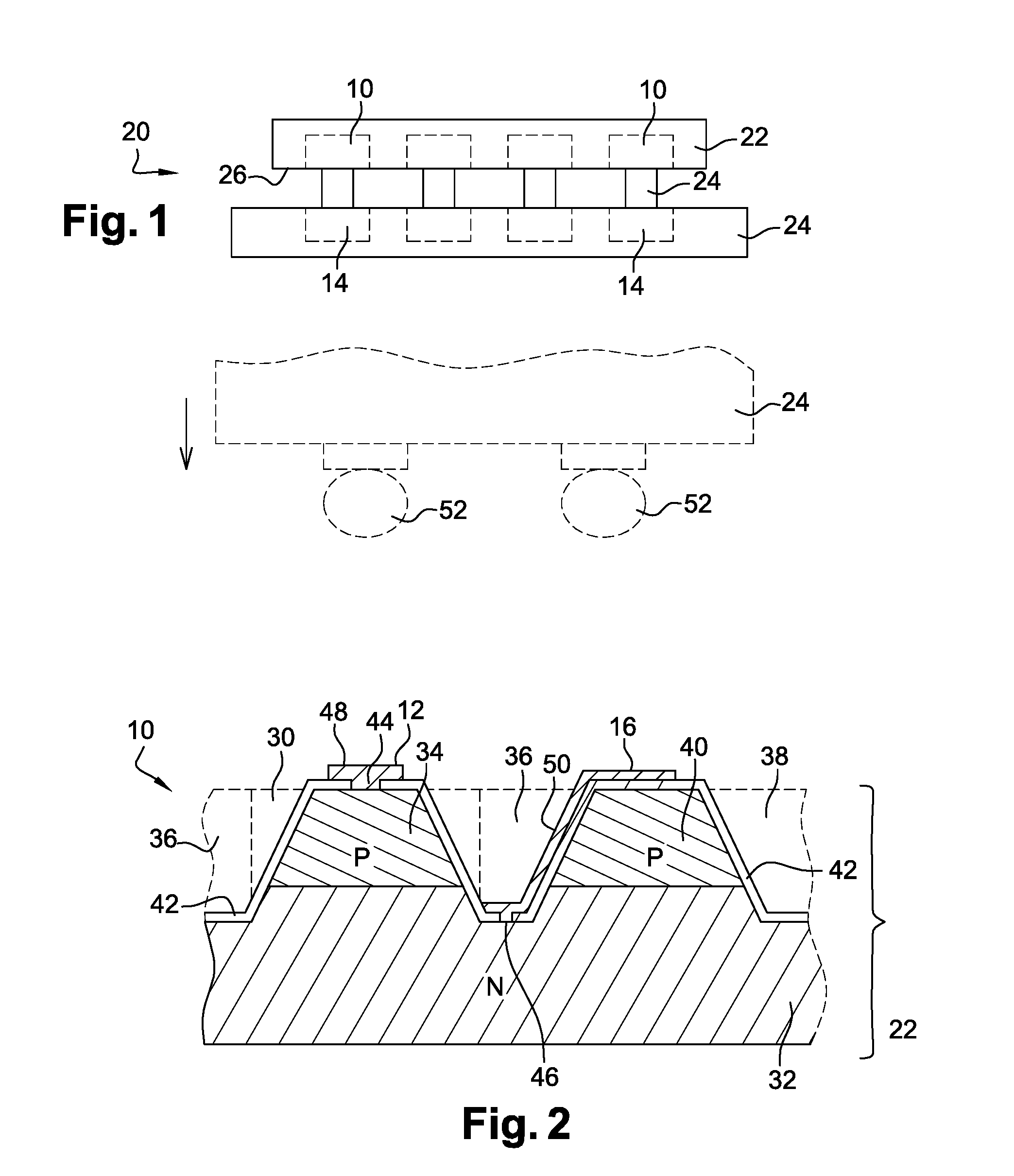
[0044]A first embodiment of the method of collective manufacturing of an array of island-shaped dipoles will now be described in relation with FIGS. 3 to 15, the array being intended to be subsequently hybridized with an external circuit for the electric connection of each dipole.

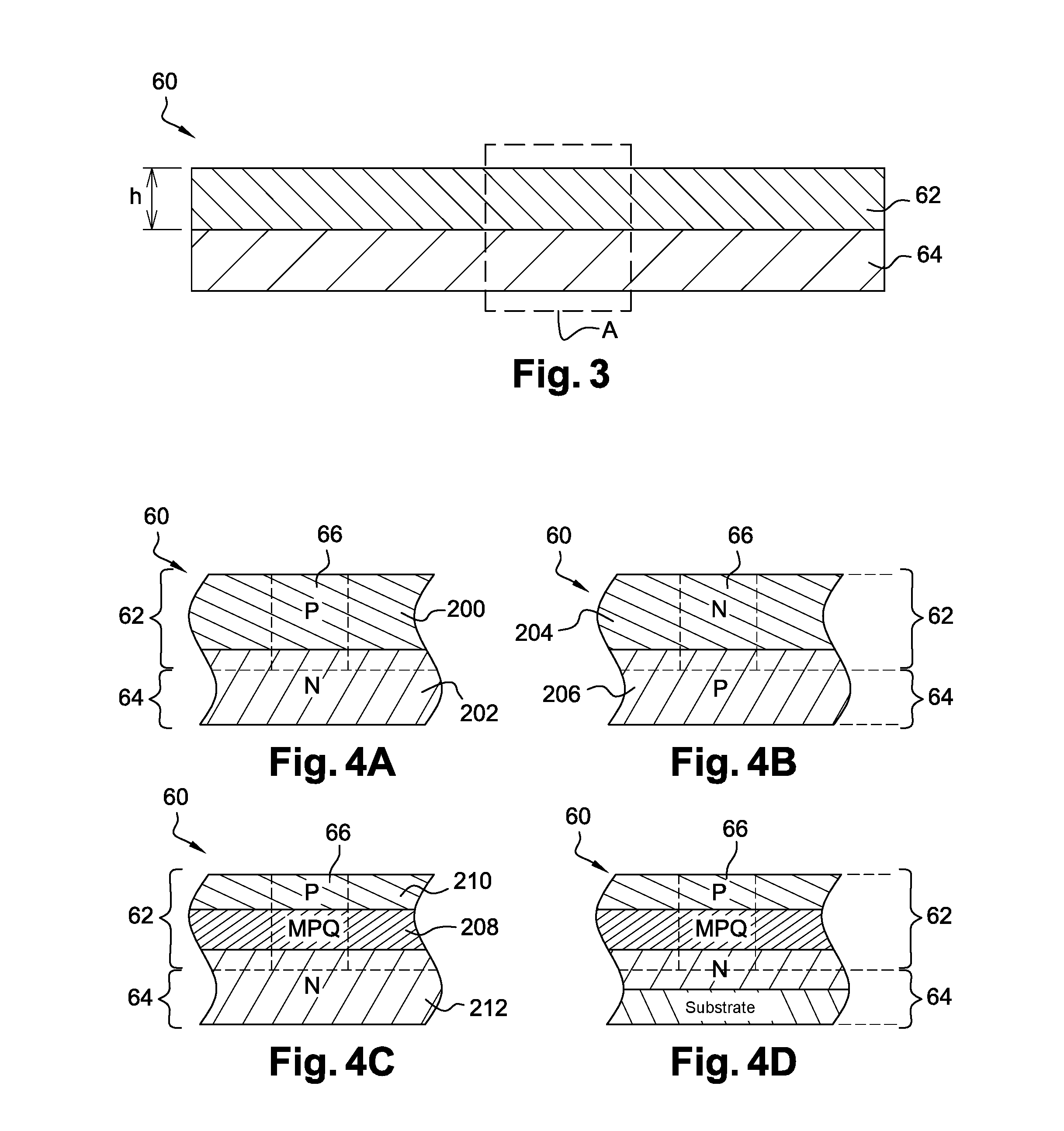
[0045]The method starts (FIG. 3) with the forming of a plate 60 containing all the active materials forming the dipoles. Plate 60 is divided between a first thickness 62 of value “h” where the islands will be formed and a second thickness 64 forming the base which will support the islands.

[0046]Plates 60 used in the context of the manufacturing of an array of photodiodes are illustrated in FIGS. 4A-4D, which are for example detail views of box A of FIG. 3.

[0047]For example (FIG. 4A), plate 60 comprises a layer 200 of N-type semiconductor material having a layer 202 of P-type semiconductor material deposited thereon, the manufacturing of the islands comprising individualizing volumes 66 formed across the ent...


PUM

PropertyMeasurementUnit
heightaaaaaaaaaa
heightaaaaaaaaaa
thicknessaaaaaaaaaa

Abstract

An electronic component includes a plurality of dipoles, each comprising an island solid with a base, a first electrode arranged at the top of the island and a second electrode arranged on the base. Its manufacturing includes forming, on the base, a layer of a material capable of being etched by means of a predetermined isotropic etching, forming, over the layer of material, solid patterns made of electrically-conductive material and inert to said etching, applying the isotropic etching of the thickness of material between said solid patterns to form islands totally overlooked by said solid patterns, and depositing electrically-conductive material on top of and between the islands to form the first and second electrodes of the dipoles.

Description

CROSS-REFERENCE TO RELATED APPLICATIONS[0001]This application claims the benefit of priority under 35 U.S.C. §119 of prior-filed French Patent Application No. 1555785, filed Jun. 24, 2015, the entire content of which is hereby incorporated herein by reference, in its entirety and for all purposes.TECHNOLOGICAL FIELD[0002]The present specification relates to the manufacturing of electronic components, and more specifically to the manufacturing of electronic components comprising on a same surface a large density of dipoles.[0003]The present specification particularly applies to devices comprising two electronic components interconnected face to face with very small interconnection pitches, by means of a “flip-chip” type hybridization method. The present specification thus specifically applies in so-called chip-on-chip, chip-on-wafer, and wafer-on-wafer assemblies. For example, the present specification applies to illumination arrays and to hybrid imagers of very large dimensions and ...

Claims


Application Information

Patent Timeline
Patent Type & Authority Applications(United States)
IPC IPC(8): H01L27/146
CPCH01L27/14632H01L27/14643H01L27/14636H01L27/14698H01L27/1462H01L27/14687H01L27/1469H01L27/14634H01L27/1446
Inventor MARION, FRANCOIS
Owner COMMISSARIAT A LENERGIE ATOMIQUE ET AUX ENERGIES ALTERNATIVES
Why Eureka
Try Eureka