Heating system comprising semiconductor light sources

a technology of semiconductor light source and heating system, which is applied in the direction of chemically reactive gas, coating, crystal growth process, etc., can solve the problems of unsatisfactory reliability and homogeneity of the heating process of the apparatus, and achieve the effect of improving the homogeneity of the temperature distribution, reducing the required heating power, and improving the reliability of the heating system

Active Publication Date: 2016-12-29
TRUMPF PHOTONIC COMPONENTS GMBH
View PDF0 Cites 313 Cited by
  • Summary
  • Abstract
  • Description
  • Claims
  • Application Information

AI Technical Summary

Benefits of technology

[0033]It may be further advantageous that the temperature distribution of the processing surface may be monitored in addition if the processing surface and the heating surface do not at least partly coincide. Monitoring the processing surface may in this case be used to further increase the homogeneity of the temperature distribution of the processing surface.
[0034]The heating system may in an advantageous embodiment comprise at least 50000, 100000, 500000 or even more semiconductor light sources. Using more semiconductor light sources for heating a heating surface of a defined area size increases the number of semiconductor light sources heating one area element of the heating surface. The reliability of the heating system may be improved because a malfunction of one semiconductor light source may be negligible in comparison to the total optical power emitted to heat the respective area element of the heating surface.
[0035]As semiconductor light sources may be expensive, it may be advantageous that the heating system may comprise a heating module for providing a first temperature distribution of heating surface of the object and the semiconductor light sources are adapted to provide a homogeneous temperature distribution at the processing temperature. The heating module may comprise conventional heating devices like, for example, halogen lamps for heating the heating surface to a temperature near to the processing temperature. The semiconductor light sources are used to compensate inhomogeneity which may be caused by the heating module and / or the geometrical boundary condition. The semiconductor light sources may be arranged in sub modules like the sub modules of the second group of sub modules as discussed above in order to compensate local differences of the temperature of the heating surface. The combination of a conventional heating module with semiconductor light sources may be cheaper than a heating system comprising only semiconductor light source. It may be a disadvantage of such a combined system that temperature measurement by means of optical temperature sensors may be disturbed by means of the broadband emission of the, for example, halogen lamps.
[0036]A reactor for wafer processing may comprise a heating system as described above and a reactor chamber, wherein the heating system is adapted to heat at least one wafer within the reactor chamber. The heating system may be positioned at the inside of the reactor chamber. It may be advantageous to separate the heating system from the object. A glass plate with a light-transmissive coating for the light emitted by the semiconductor light sources but reflective for longer wavelengths thermal radiation from the object may facilitate as thermal separation thus reducing the required heating power. A further separation may avoid a direct gas flow between the reactor chamber and the semiconductor light sources of the heating system. This may be realized by a membrane like construction and two separate vacuum systems but still inside the reactor chamber i.e. at the same low pressure.
[0037]Alternatively, it may be advantageous to arrange the heating system outside the reactor chamber. The reactor chamber may comprise in this case at least one reactor window, and the heating system is adapted to heat the wafer by irradiating light via the reactor window. A complete separation of the heating system from the reactor chamber may have the advantage that, for example, the heating system has not to be adapted to the conditions in the reactor chamber. Furthermore, maintenance operations which are only related to the heating system may be independent from the reactor chamber such that, for example, the vacuum within the reactor chamber can be maintained. Recalibration of the deposition system as, for example, in a MOCVD or MBE reactor may not be necessary such that the time needed for the maintenance operation may be reduced.

Problems solved by technology

The reliability and homogeneity of the heating process of the apparatus is still unsatisfactorily.

Method used


Image

  • Heating system comprising semiconductor light sources
  • Heating system comprising semiconductor light sources
  • Heating system comprising semiconductor light sources

Examples


first embodiment

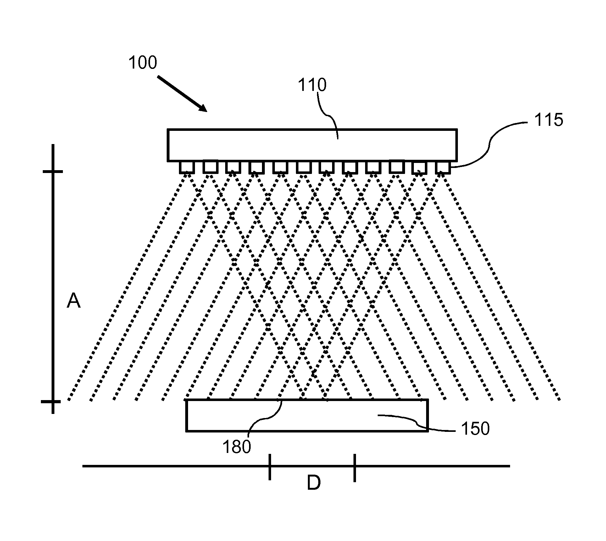
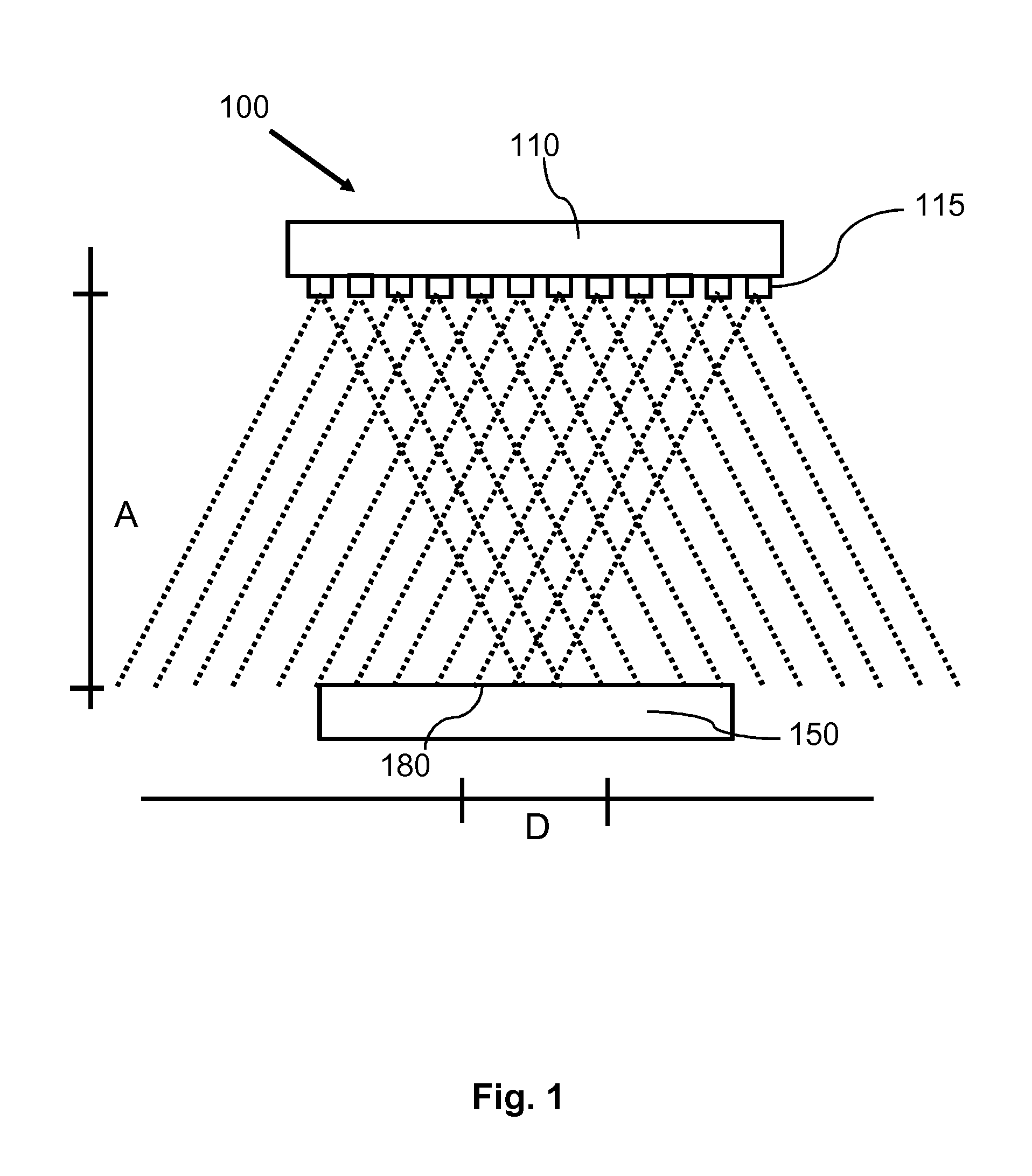
[0075]FIG. 1 shows a principal sketch of a cross section of a heating system 100. The heating system comprises one sub module 110 with a multitude of semiconductor light sources 115 like VCSEL. The VCSEL emit laser light to an object 150 with a heating surface 180 with a diameter D at a distance A to the light emitting surface of the VCSEL. The heating surface 180 does not cover the entire upper surface of the object 150 next to the VCSEL. The distance A, the pitch between the VCSELs and the halve divergence angle a of the VCSEL are arranged such that an area element of the heating surface 180 is illuminated by means of at least 50 VCSEL. The divergence angle is defined as the angle where the intensity emitted by a semiconductor light source is reduced to 1 / e2 of the maximum intensity emitted by specific light source (e Euler number 2,71 . . . ).

[0076]For a square arrangement of the light sources with the pitch p this can be achieved by fulfilling the equation π (A tan α)2>50p2. The...

second embodiment

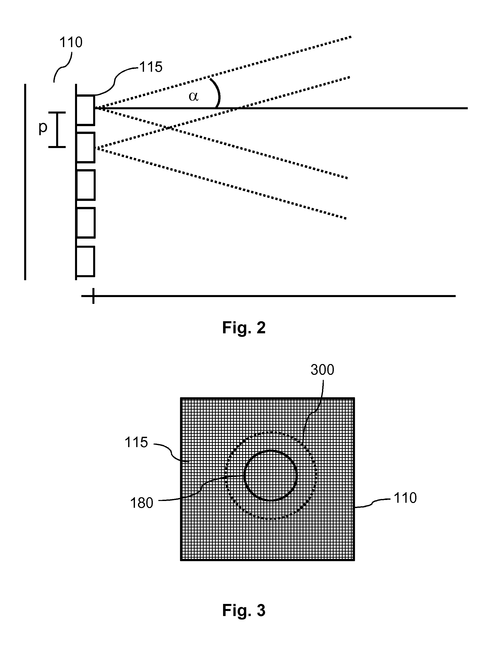
[0080]FIG. 3 shows a principal sketch of a heating system 100. The heating system 100 is shown from the perspective of the heating surface 180 of the object 150. The area 300 of the heating surface 180 illuminated by one semiconductor light source 115 is indicated by the dotted circle representing the line at which 1 / e2 of the maximum intensity received by the heating surface from the respective semiconductor light source is received. The semiconductor light sources 115 are indicated as squares on the sub module 110. Taking an area element near or at the center of the heating surface 180 (e.g. one of the squares),it's obvious that the light emitted by much more than 50 semiconductor light sources 115 overlaps at the respective area element of the heating surface 180. The minimum size of the sub module 110 in order to provide a homogeneous illumination has in this embodiment to be at least equal to the sum of the diameter of the heating surface 180 and the diameter of the area 300. L...

third embodiment

[0081]FIG. 4 shows a principal sketch of a cross section of a heating system. FIG. 5 shows a top view of the heating system 100 shown in FIG. 4 wherein the dashed line 510 indicates the line of the cross section shown in FIG. 4. Two groups of sub modules 110 with a multitude of semiconductor light sources are shown. Each sub module 110 of the first group of sub modules 410 emits light covering the whole heating surface 180 of the object 150 as indicated by the dotted lines. An idealized example of an intensity profile 620 provided by a sub module 110 of the first group of sub modules 410 is shown in FIG. 6. The intensity is essentially constant across the diameter D of the heating surface 180. In reality the intensity profile may be trapezoidal such that the area of constant intensity has to cover the whole heating surface 180. The sub modules 110 of the second group of sub modules 420 emits light covering only parts of the heating surface 180 of the object 150 as indicated by the d...


PUM

PropertyMeasurementUnit
processing temperatureaaaaaaaaaa
temperatureaaaaaaaaaa

Abstract

The invention describes a heating system (100) and a corresponding method of heating a heating surface (180) of an object (150, 950) to a processing temperature of at least 100° C., wherein the heating system (100) comprises semiconductor light sources (115), and wherein the heating system (100) is adapted to heat an area element of the heating surface (180) with at least 50 semiconductor light sources (115) at the same time. The heating system (100) may be part of a reactor for processing semiconductor structures. The light emitted by means of the semiconductor light sources (115) overlaps at the heating surface (180). Differences of the characteristic of one single semiconductor light source (115) may be blurred at the heating surface (180) such that a homogeneous temperature distribution across a processing surface of a, for example, wafer may be enabled.

Description

FIELD OF THE INVENTION[0001]The invention relates to a heating system comprising semiconductor light sources for directly or indirectly heating an object like an OLED substrate, a semiconductor wafer or the like. The invention further relates to a corresponding method of heating the object.BACKGROUND OF THE INVENTION[0002]Deposition of organic and inorganic semiconductor structures needs as homogeneous temperature distribution as possible. Variations of the processing temperature of some degree across, for example, a semiconductor wafer changes the growth conditions and thus the characteristics of the grown semiconductor layer. An example is the growth of LEDs emitting visible light on the basis of GaN. The growth temperature above 1000° C. has to be maintained within 0.5° C. in order to avoid wavelength shifts of the LEDs which in consequence require costly binning of products.[0003]U.S. Pat. No. 8,222,574 B2 discloses, for example, an apparatus and a corresponding method for achie...

Claims


Application Information

Patent Timeline
Patent Type & Authority Applications(United States)
IPC IPC(8): H05B3/00H01L51/56C30B25/10C23C16/48C23C16/46C30B23/06H01L21/67H05B1/02
CPCH05B3/0047H01L21/67115H01L51/56C30B25/105C23C16/481C23C16/46C30B23/063H05B1/0233H10K71/00
Inventor MOENCH, HOLGERDERRA, GUENTHER HANSGRONENBORN, STEPHANPEKARSKI, PAVELKOLB, JOHANNA SOPHIECONRADS, RALF GORDON
Owner TRUMPF PHOTONIC COMPONENTS GMBH
Why Eureka
Try Eureka