Semiconductor wafer processing methods and apparatus

a technology of semiconductors and wafers, applied in semiconductor/solid-state device testing/measurement, instruments, transportation and packaging, etc., can solve the problems of reducing the accuracy and corresponding errors in the weight measurement performed by the weighing apparatus. , to achieve the effect of reducing the thermal contact area, and reducing the temperature of the weighing apparatus

Active Publication Date: 2017-01-05
METRYX
View PDF2 Cites 5 Cited by
  • Summary
  • Abstract
  • Description
  • Claims
  • Application Information

AI Technical Summary

Benefits of technology

[0120]The apparatus may comprise a further semiconductor wafer transporter for transporting the semiconductor wafer on to the temperature changing unit before the semiconductor wafer is transported from the temperature changing unit to the processing area of the semiconductor wafer processing apparatus. For example the first semiconductor wafer transporter may be a first end effector and the further semiconductor wafer transporter may be a second end effector. Using separate wafer transporters (e.g. end effectors) may be advantageous as it may mean that the temperatures of the wafer transporters are more closely matched to the temperatures of the semiconductor wafers that they are used to transport. The semiconductor wafer transporter used to transport a semiconductor wafer from a FOUP to the thermal transfer plate might be relatively hot, because the wafers in the FOUP might be hot (e.g. they may be approximately 70° C.). If the same semiconductor wafer transporter is used to transport the semiconductor wafer from the thermal transfer plate to the processing area after the wafer has been cooled (e.g. to 20° C.) the semiconductor wafer transporter may transfer heat to the semiconductor wafer and increase its temperature. This may be avoided by using a different semiconductor wafer

Problems solved by technology

This heat load may cause the temperature of the weighing apparatus (e.g. the temperature of a balance of the weighing apparatus) to increase or to become non-uniform, which may cause corresponding errors in the weight measurements performed by the weighing apparatus.
In addition, this heat load can cause air currents (e.g. convection currents) and changes in the air density and pressure around the

Method used


Image

  • Semiconductor wafer processing methods and apparatus
  • Semiconductor wafer processing methods and apparatus
  • Semiconductor wafer processing methods and apparatus

Examples


first embodiment

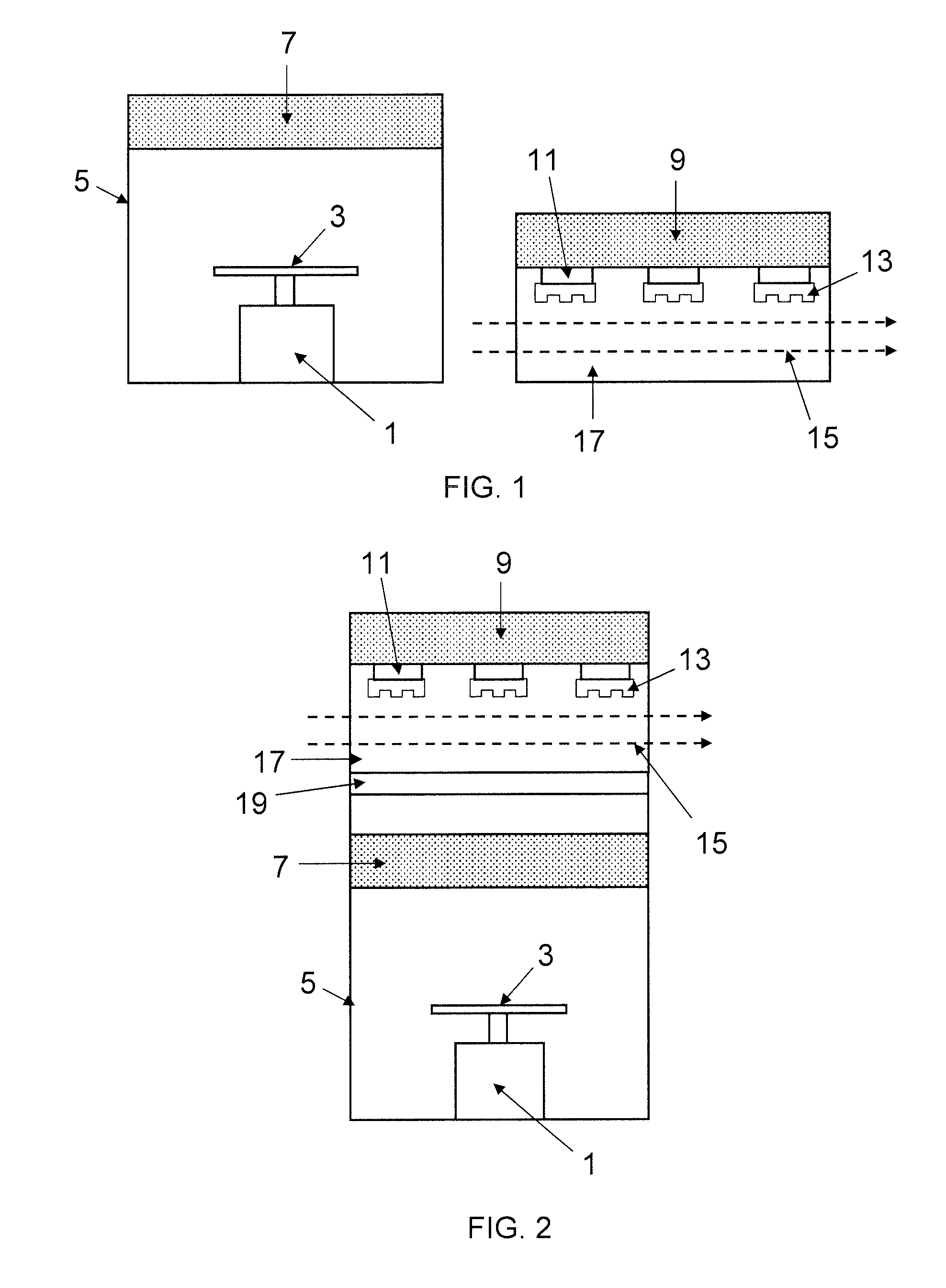
[0129]FIG. 1 shows a weighing apparatus according to the present invention. The weighing apparatus comprises a weighing balance 1 having a weighing pan 3 for receiving a semiconductor wafer. The weighing balance 1 is configured to provide measurement output indicative of the weight of a semiconductor wafer loaded on the weighing pan 3.

[0130]The weighing balance 1 is located within a weighing chamber 5, which forms an enclosed environment around the weighing balance 1, e.g. to maintain a substantially uniform air density, air pressure and air temperature of the air around the weighing balance and to prevent draughts and provide electromagnetic shielding. The weighing chamber 5 has an opening (not shown), e.g. a suitably sized slot in a side-wall of the weighing chamber 5, to allow a semiconductor wafer to be transported into the weighing chamber 5, e.g. by a robotic arm, and positioned on the weighing pan 3. When not in use, the opening may be covered by an openable door or covering ...

second embodiment

[0151]FIG. 2 shows a weighing apparatus according to the present invention. Similar or corresponding features to those present in FIG. 1 are indicated using the same reference numerals as used in FIG. 1, and description of those features is not repeated.

[0152]The primary difference between the first and second embodiments is the positioning of the thermal transfer plate 9. In the second embodiment, the thermal transfer plate 9 is stacked above the thermal transfer plate 7. A thermal gap 19, for example an air gap or a layer of insulating material, is positioned between the thermal transfer plate 7 and the thermal transfer plate 9, so that the thermal transfer plates 7, 9 are substantially thermally insulated from each other so that substantially no heat can pass between the thermal transfer plates 7, 9.

[0153]Floor space is often limited in semiconductor device production facilities. Therefore, it may be advantageous to stack the thermal transfer plate 9 above the thermal transfer pl...
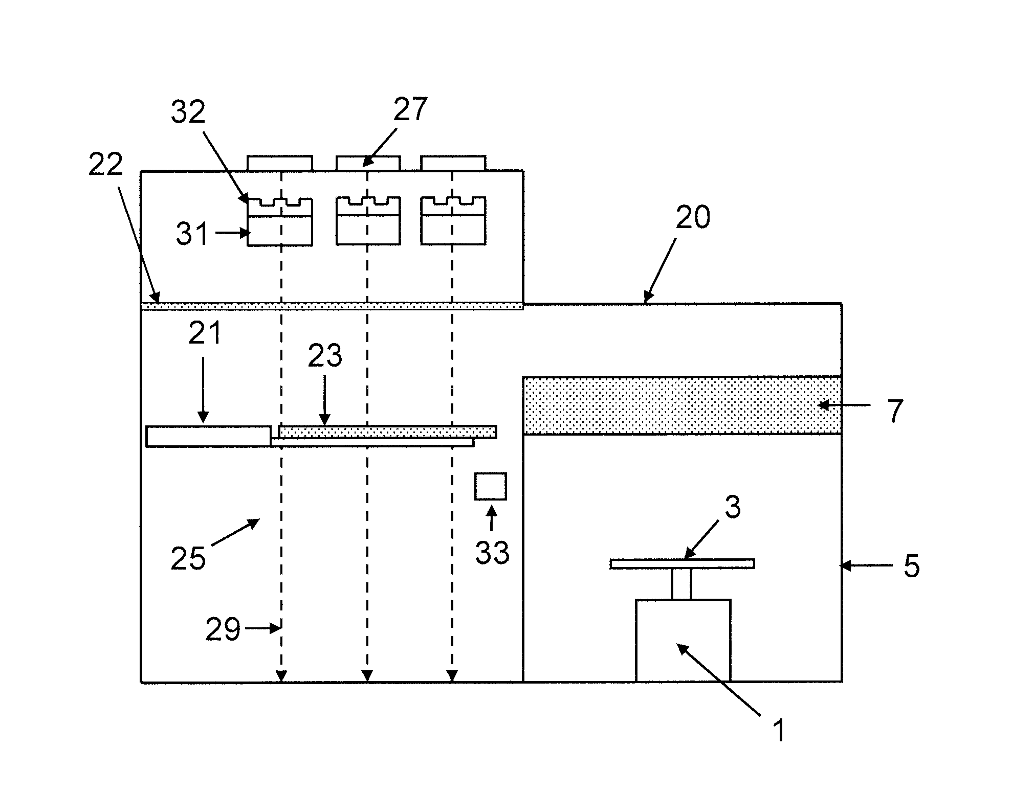
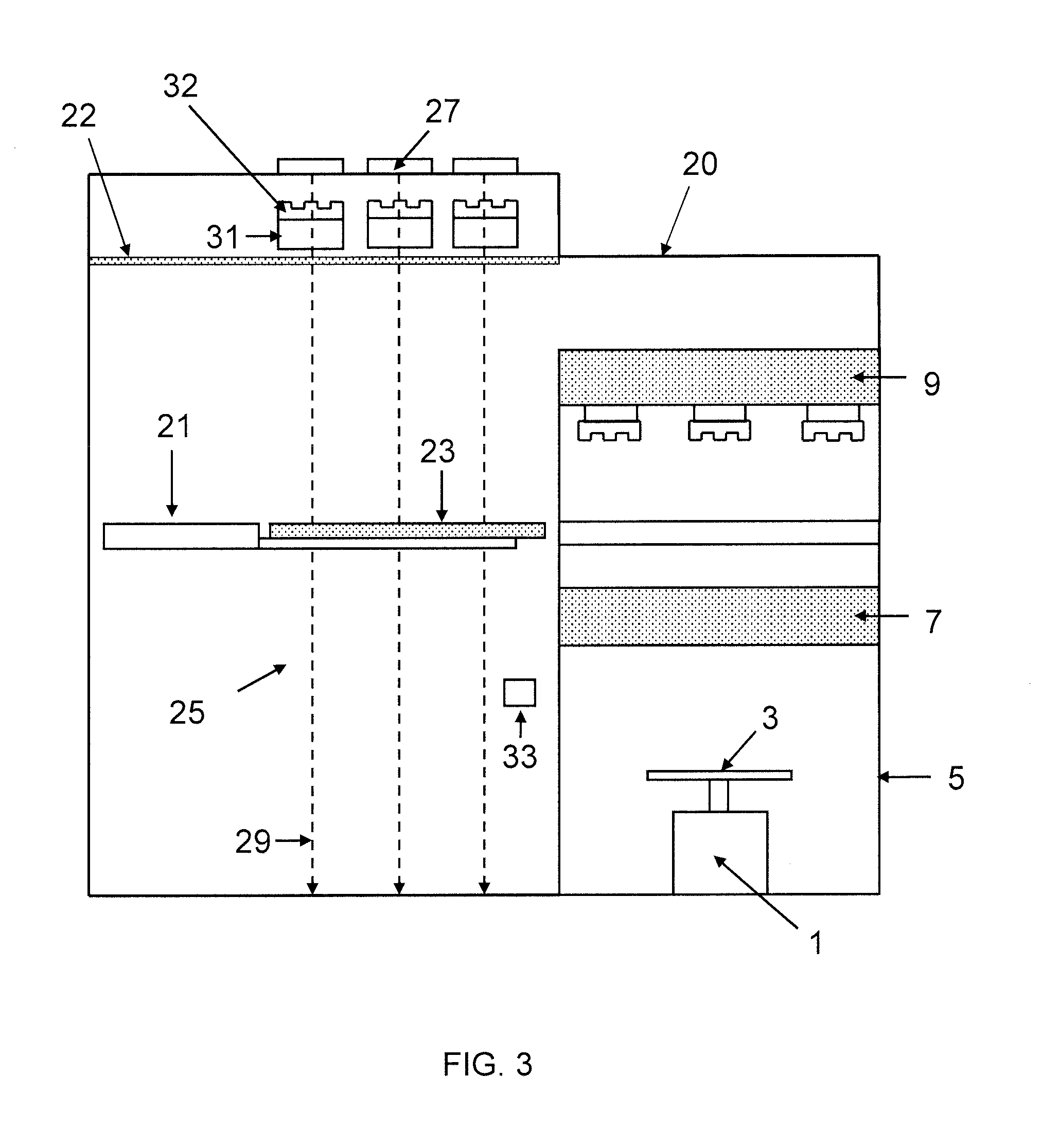
third embodiment

[0154]FIG. 3 shows a weighing apparatus according to the present invention including a wafer transportation system. Similar or corresponding features to those present in FIG. 1 are indicated using the same reference numerals as used in FIG. 1, and description of those features is not repeated. As shown in FIG. 3, the weighing apparatus and wafer transportation system are enclosed in an EFEM enclosure 20, within which a clean room environment is maintained / generated. As shown in FIG. 3, the wafer transportation system comprises one or more end effectors 21 of a robotic arm, for example a robotic arm of an EFEM. The end effector 21 is used to hold or support a semiconductor wafer 23 and to transport the semiconductor wafer 23 between the different parts of the weighing apparatus, e.g. between the thermal transfer plate 9, the thermal transfer plate 7 and the weighing pan 3.

[0155]As shown in FIG. 3, when the end effector 21 transports the semiconductor wafer 23 it transports the semico...


PUM


Abstract

A semiconductor wafer processing method comprising controlling the temperature of a semiconductor wafer to be within a predetermined processing temperature range by: causing a first temperature change of the semiconductor wafer using a first temperature changing unit; and subsequently causing a second temperature change using a second temperature changing unit; wherein the first change is greater than the second change; and subsequently loading the semiconductor wafer on a processing area of a semiconductor wafer processing apparatus. Also, a semiconductor wafer processing method comprising controlling the temperature of a semiconductor wafer to be within a predetermined processing temperature range by causing a temperature change of the semiconductor wafer using a temperature changing unit; transporting the semiconductor wafer from the temperature changing unit to a processing area of a semiconductor wafer processing apparatus; and controlling the temperature of the semiconductor wafer during the transporting step.

Description

FIELD OF THE INVENTION[0001]The present invention relates to a semiconductor wafer processing method, for example a semiconductor wafer metrology method.[0002]The present invention also relates to a semiconductor wafer processing apparatus, for example a semiconductor wafer metrology apparatus.BACKGROUND OF THE INVENTION[0003]Microelectronic devices are fabricated on semiconductor (e.g. silicon) wafers using a variety of techniques, e.g. including deposition techniques (CVD, PECVD, PVD, etc.) and removal techniques (e.g. chemical etching, CMP, etc.). Semiconductor wafers may be further treated in ways that alter their mass, e.g. by cleaning, ion implantation, lithography and the like.[0004]Depending on the device being manufactured, each semiconductor wafer may be passed sequentially through hundreds of different processing steps to build up and / or to remove the layers and materials necessary for its ultimate operation. In effect, each semiconductor wafer is passed down a production...

Claims


Application Information

Patent Timeline
IPC IPC(8): H01L21/66H01L21/677H01L21/67
CPCH01L21/67109H01L21/67248H01L21/67253H01L21/67748H01L21/67103G01G23/00G01G23/48H01L21/67706H01L22/26
Inventor WILBY, ROBERT JOHNKIERMASZ, ADRIAN
Owner METRYX
Why Eureka
Try Eureka