Semiconductor device and method for fabricating the same

a technology of semiconductor devices and contact plugs, which is applied in the direction of semiconductor devices, semiconductor/solid-state device details, electrical apparatus, etc., can solve the problems of poor accuracy affecting the interconnection of contact plugs and overall performance of the device, the integration of metal gates and contact plugs still faces some problems in conventional finfet fabrication, and achieves the effect of dramatic increasing the integration

Active Publication Date: 2017-01-12
UNITED MICROELECTRONICS CORP
View PDF4 Cites 30 Cited by
  • Summary
  • Abstract
  • Description
  • Claims
  • Application Information

AI Technical Summary

Benefits of technology

[0008]The semiconductor device and the forming method thereof in the present invention utilizes adjusting the forming time of the trench and selectively forming the spacer layer on the sidewalls of the trench to shrink the critical dimension of the trench such that one single dummy gate structure is allowed to stretch over the etched edges of two adjacent fin structures and the trench between the two adjacent fin structures, thereby dramatically increasing the integration. Through such arrangement, it is sufficient to avoid the critical dimension of the trench opening being enlarged due to overreaction with or over-consumption by oxygen provided in the forming processes of the shallow trench isolation or the dielectric layer, such as the flowable chemical vapor deposition process or the thermal oxidization process.

Problems solved by technology

However, integration of a metal gate and contact plugs still faces some issues in conventional FinFET fabrication.
For instance, issues such as tiger tooth often arise when contact holes are formed with poor accuracy influencing the interconnection of contact plugs and overall performance of the device.

Method used


Image

  • Semiconductor device and method for fabricating the same
  • Semiconductor device and method for fabricating the same
  • Semiconductor device and method for fabricating the same

Examples


first embodiment

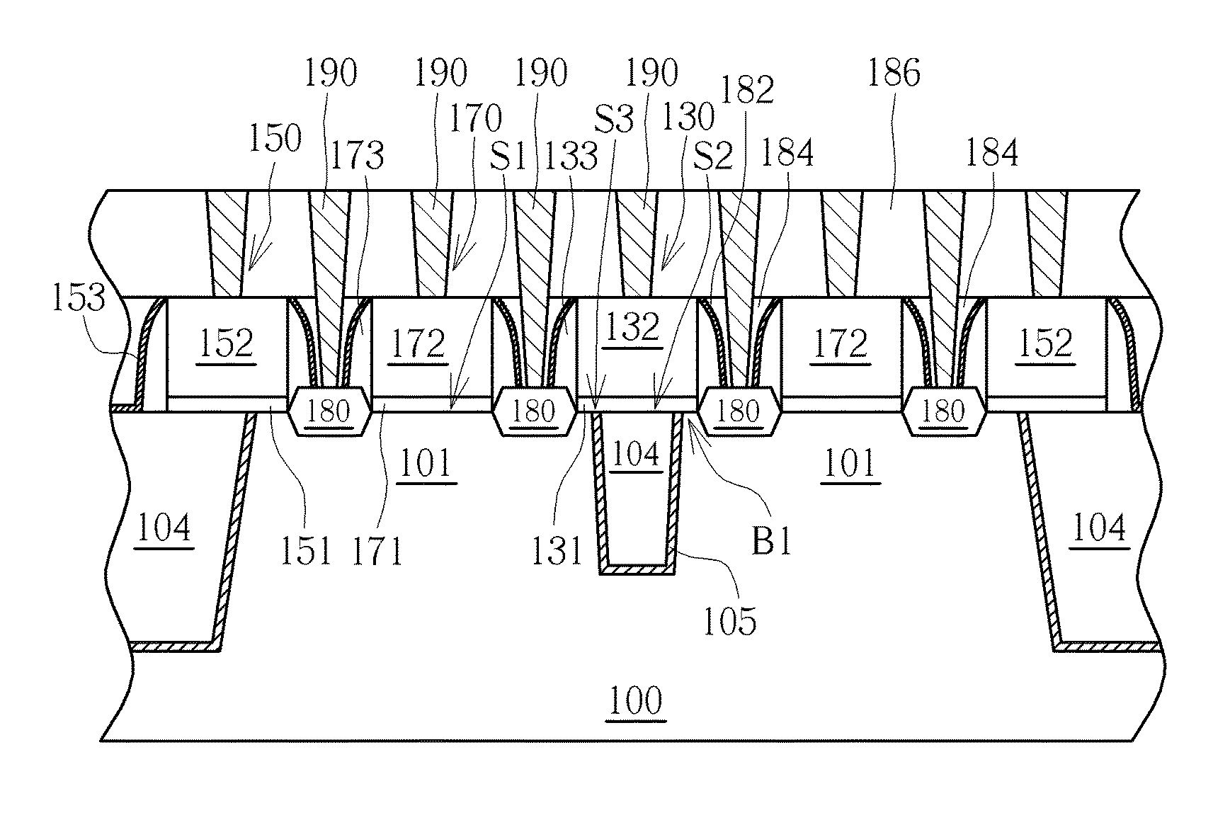
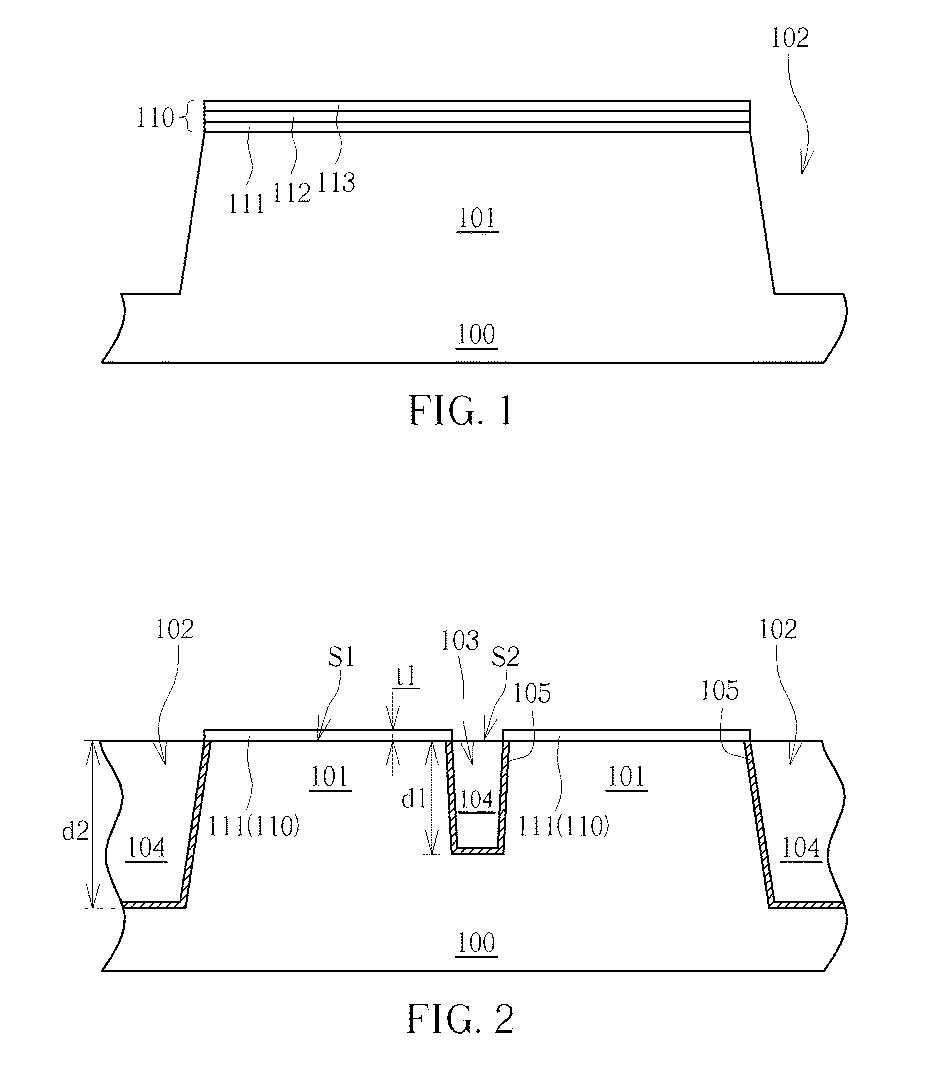
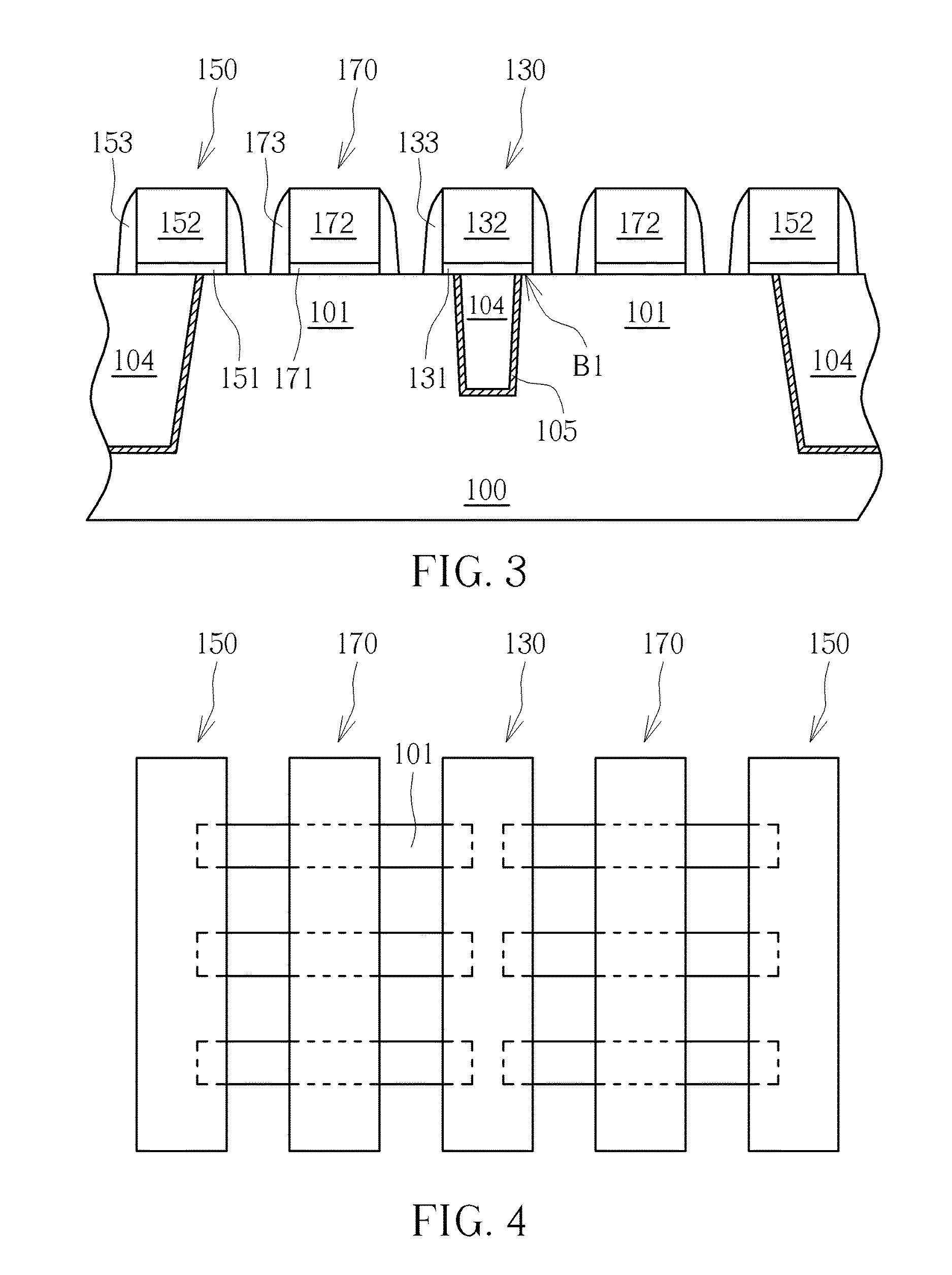
[0016]Please refer to FIG. 1 to FIG. 6, which are schematic diagrams illustrating a method of forming a semiconductor device according to the present invention, wherein FIG. 4 shows a top view of the semiconductor device in forming steps. First of all, as shown in FIG. 1, a substrate 100 is provided, the substrate 100 for example includes a semiconductor substrate, such as a silicon substrate, a silicon-containing substrate or a silicon-on-insulator (SOI) substrate, and at least one fin structure 101 is formed in the substrate 100. In an example of bulk silicon, the fin structures 101 may be formed preferably through a sidewall image transfer (STI) process. The process may include forming a plurality of patterned sacrificial layers (not shown in the drawings) on the substrate 100 by using a photolithography and an etching process, performing a depositing and an etching processes sequentially to form a spacer (not shown in the drawings) at sidewalls of each of the patterned sacrifici...

second embodiment

[0033]Please refer to FIG. 7 to FIG. 8, which are schematic diagrams illustrating a method of forming a semiconductor device according to the present invention. The difference between this embodiment and the first preferred embodiment mentioned above is that the material of the insulating layer 104′ in the trench 103 is different from that of the insulating layer 104 in the trench 102. Preferably, the insulating layer 104 can be formed of materials such as silicon oxide, and the insulating layer 104′ can be formed of materials such as silicon nitride, but not limited thereto. In addition, the top surface of the insulating layer 104 (also the top surface of the STI) is lower than the top surface of the fin structure 101 or the top surface of the insulating layer 104′. Therefore, the gate structure 170 formed in the following steps can still cover on the top surface and two sidewalls of the fin structure 101, thereby increasing the channel width of the device. Other features in this e...

third embodiment

[0035]In addition, please refer to FIG. 9, which is schematic diagrams illustrating a method of forming a semiconductor device according to the present invention. In this embodiment the depth of the insulating layer 104″ is deeper than that of the trench 102. Other features in this embodiment are similar to that of the second preferred embodiment mentioned above, and will not be redundantly described here.


PUM


Abstract

A semiconductor device and a method of fabricating the same, the semiconductor device including a fin structure, a first liner, a first insulating layer and a dummy gate structure. The fin structure is disposed on a substrate, where the fin structure has a trench. The first liner disposed in the trench. The first insulating layer disposed on the first liner. The dummy gate structure is disposed on the first insulating layer and disposed above the trench, where a bottom surface of the dummy gate and a top surface of the fin structure are on a same level.

Description

BACKGROUND OF THE INVENTION[0001]1. Field of the Invention[0002]The invention relates to a semiconductor device and a method of forming the same, and more particularly, to a semiconductor device having a dummy gate structure and a method of forming the same.[0003]2. Description of the Prior Art[0004]With the trend in the industry being towards scaling down the size of the metal oxide semiconductor transistors (MOS), three-dimensional or non-planar transistor technology, such as fin field effect transistor technology (FinFET) has been developed to replace planar MOS transistors. Since the three-dimensional structure of a FinFET increases the overlapping area between the gate and the fin structure of the silicon substrate, the channel region can therefore be more effectively controlled. This way, the drain-induced barrier lowering (DIBL) effect and the short channel effect are reduced. The channel region is also longer for an equivalent gate length, thus the current between the source...

Claims


Application Information

Patent Timeline
Patent Type & Authority Applications(United States)
IPC IPC(8): H01L23/535H01L29/16H01L29/06H01L29/161H01L29/66H01L29/78
CPCH01L23/535H01L29/6681H01L29/66515H01L29/1608H01L29/0653H01L29/161H01L29/7851H01L29/66795H01L29/785H01L23/485H01L29/165H01L21/823431H01L27/0886H01L21/76805H01L21/76895H01L21/823475H01L21/823481H01L29/0649H01L29/66545
Inventor TSENG, I-MINGLIANG, WEN-ANHUANG, CHEN-MING
Owner UNITED MICROELECTRONICS CORP
Why Eureka
Try Eureka