

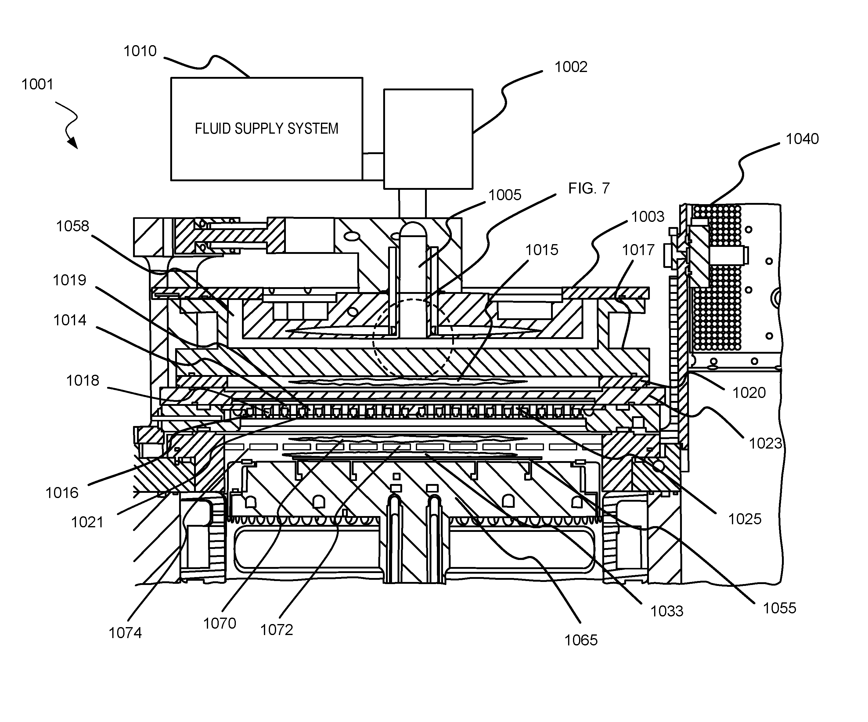
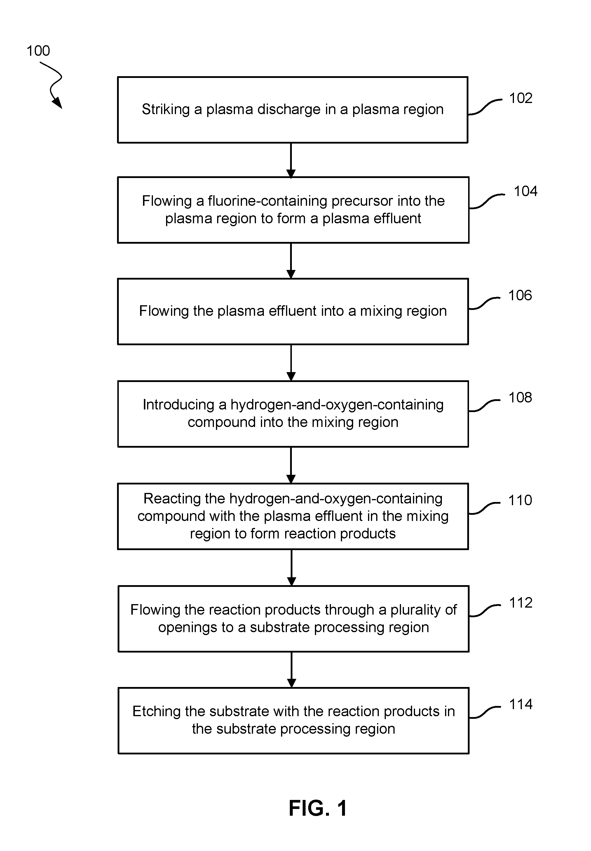
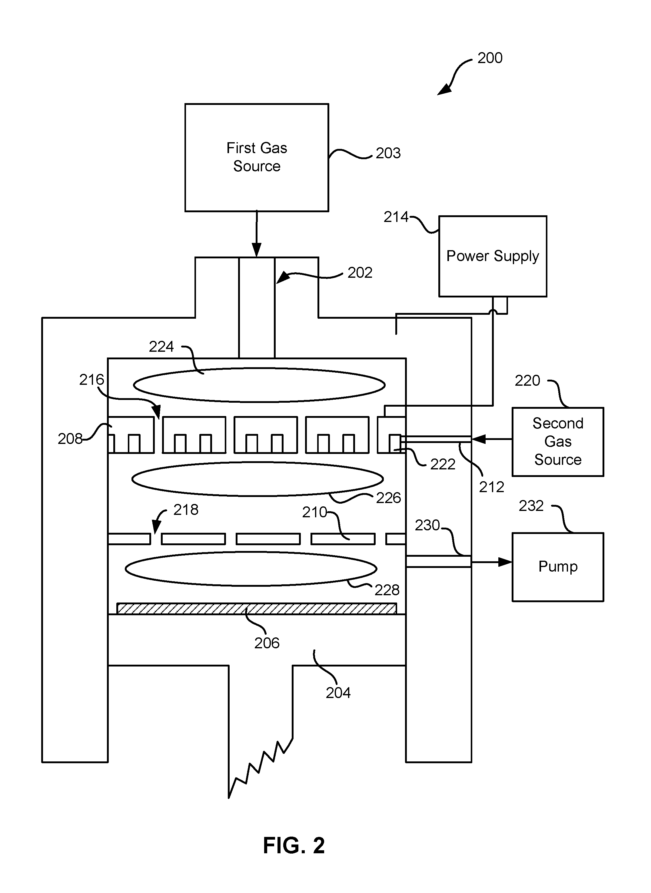
Oxide etch selectivity systems and methods
a technology of selective etching and silicon oxide, applied in the field of system and method for etching semiconductor materials, can solve the problems of undesired etching of the second material, and achieve the effects of high selective etching selectivity of silicon oxide, enhanced or suppressed reactions, and increased residence time and/or mixing
- Summary
- Abstract
- Description
- Claims
- Application Information
AI Technical Summary
Benefits of technology
Problems solved by technology
Method used
Image

Examples
example
[0044]Etch methods with a distribution plate were tested for etch selectivity against other processes without a distribution plate. Results for the various methods are shown in FIG. 5. The results for the first column is the control recipe for etching oxide. The bars indicate that the etch selectivity of oxide to polysilicon is greater than 200 and the etch selectivity of oxide to low pressure silicon nitride (“LP SiN”) is about 100. The second column of FIG. 5 shows results for an etch process termed uSMD, which includes a different ion suppressor, where the ion suppressor has a different distribution of openings and / or diameters of the openings. SMD stands for selectivity modulation device, which is an ion suppressor. The third column shows the showerhead with the uSMD distribution of openings and a recipe including helium. The results show a slight increase in etch selectivity of oxide to polysilicon and about the same etch selectivity of oxide to low pressure silicon nitride. Ho...
PUM
| Property | Measurement | Unit |
|---|---|---|
| electrically conductive | aaaaa | aaaaa |
| radius | aaaaa | aaaaa |
| circumference | aaaaa | aaaaa |
Abstract
Description
Claims
Application Information