GOA circuit based on p-type thin film transistor

a thin film transistor and circuit technology, applied in the field of display technology, can solve the problems of poor stability and higher power consumption, and achieve the effects of reducing the number of signal lines, reducing circuit power consumption, and easing the deterioration of thin film transistors

Active Publication Date: 2017-02-16
TCL CHINA STAR OPTOELECTRONICS TECH CO LTD
View PDF13 Cites 13 Cited by
  • Summary
  • Abstract
  • Description
  • Claims
  • Application Information

AI Technical Summary

Benefits of technology

[0006]An objective of the present invention is to provide a GOA circuit based on P-type thin film transistor can ease the deterioration of the thin film transistors in the forward-backward scan module, and reduce the circuit power consumption to decrease the number of the signal lines and realize the narrow frame design, and meanwhile to promote the stability of the GOA circuit.

Problems solved by technology

However, the GOA circuit based on P-type thin film transistor according to prior art often has worse stability and the power consumption is higher.

Method used


Image

  • GOA circuit based on p-type thin film transistor
  • GOA circuit based on p-type thin film transistor
  • GOA circuit based on p-type thin film transistor

Examples


first embodiment

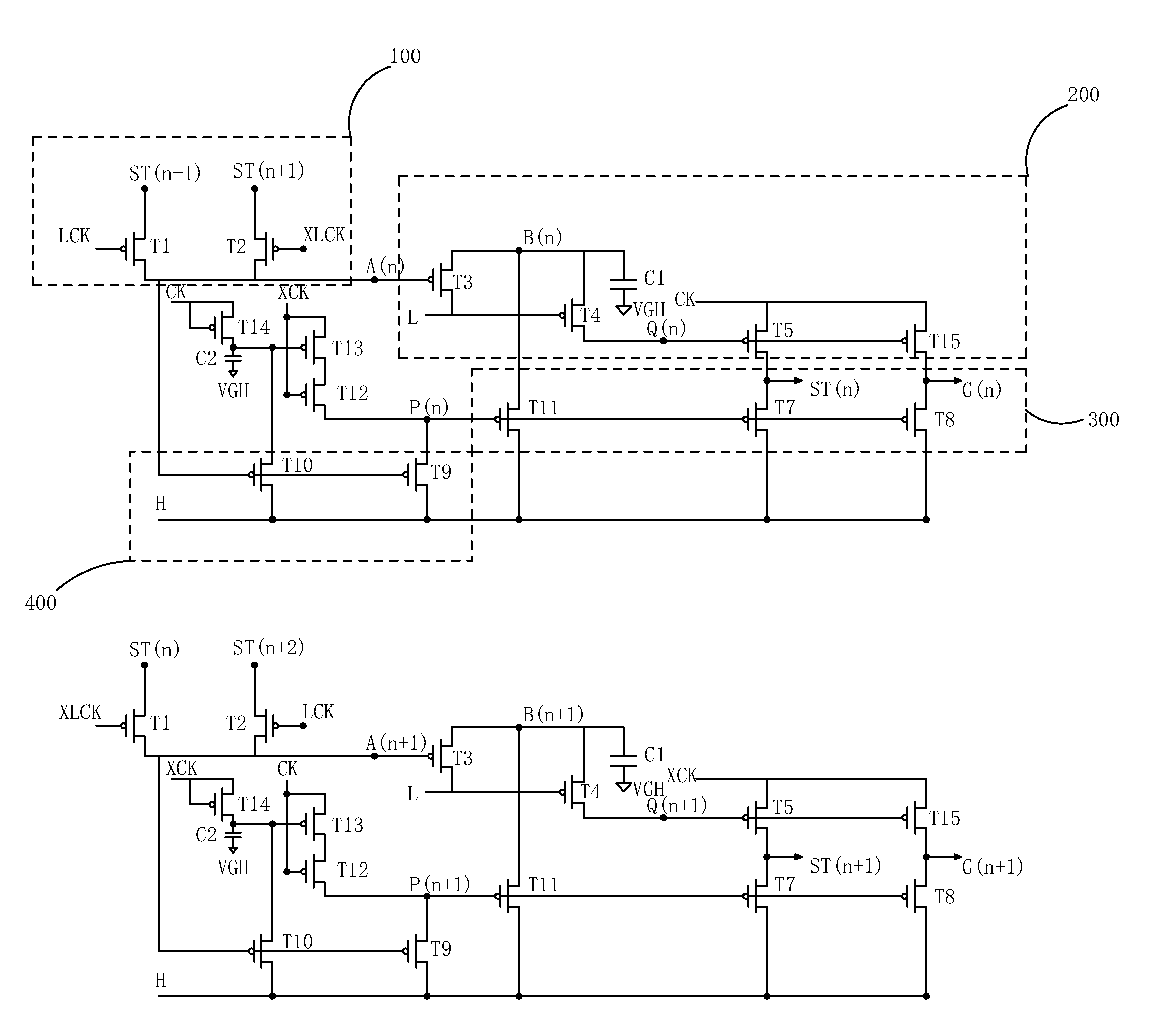
[0055]Please refer to FIG. 1. FIG. 1 is a circuit diagram of a GOA circuit based on P-type thin film transistor according to the present invention. As shown in FIG. 1, the GOA circuit based on P-type thin film transistor according to the present invention comprises a plurality of GOA unit circuits which are cascade connected, and the GOA unit circuit of every stage comprises a forward-backward scan module 100, an output module 200, a pull-down holding module 300 and a pull-down module 400. n is set to be a positive integer, and the GOA unit circuit of the nth stage and the GOA unit circuit of the n+1th stage adjacent thereto are one cycle.

[0056]Except the GOA unit circuit of the first and last stages, in the GOA unit circuit of the nth stage:

[0057]the forward-backward scan module 100 comprises: a first P-type thin film transistor T1, and a gate of the first P-type thin film transistor T1 is electrically coupled to a first high frequency clock signal LCK, and a source is electrically...

second embodiment

[0072]Please refer to FIG. 4. FIG. 4 is a circuit diagram of the second embodiment according to the present invention. Because the time sequences of the first high frequency clock signal LCK and the second backward high frequency clock signal XCK are consistent, and the time sequences of the first backward high frequency clock signal XLCK and the second high frequency clock signal CK are consistent in forward scan, thus, as performing forward scan, the second backward high frequency clock signal XCK can be replaced by the first high frequency clock signal LCK, and the second high frequency clock signal CK can be replaced by the first backward high frequency clock signal XLCK; but the time sequences of the first high frequency clock signal LCK and the second high frequency clock signal CK are consistent, and the time sequences of the first backward high frequency clock signal XLCK and the second backward high frequency clock signal XCK are consistent in backward scan, thus, as perfor...

third embodiment

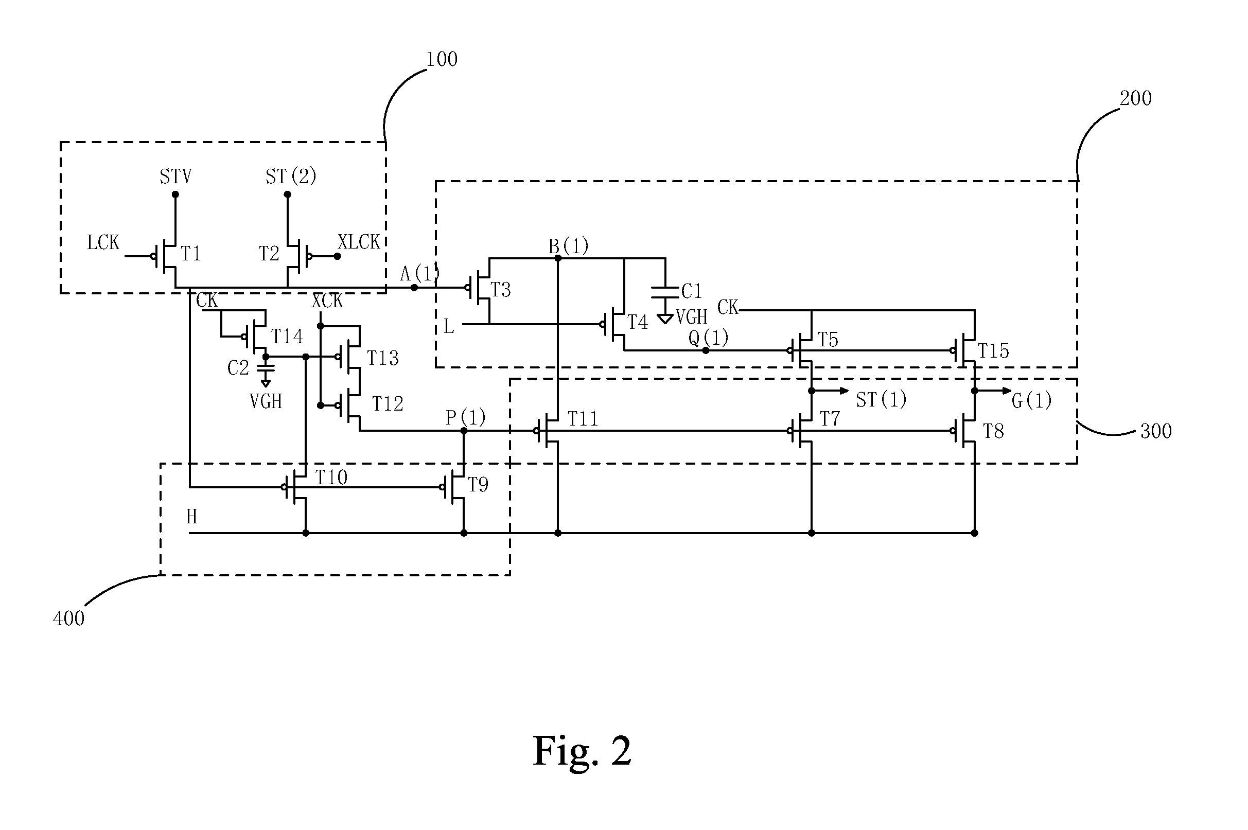
[0073]Please refer to FIG. 5. FIG. 5 is a circuit diagram of the third embodiment according to the present invention. The difference of FIG. 5 and FIG. 1 is that the GOA unit circuit of every stage further comprises a sixteenth P-type thin film transistor T16, and a gate of the sixteenth P-type thin film transistor T16 is electrically coupled to a stage transfer signal ST(n), and a source is electrically coupled to the fourth node P(n), and a drain is electrically coupled to the constant high voltage level H. In the output period, the scan signal G(n) is low voltage level, and the sixteenth P-type thin film transistor T16 is on to raise the voltage level of the fourth node P(n) to ensure that P point is stably at high voltage level to promote the output quality of the scan signal G(n). After the output is finished, the sixteenth P-type thin film transistor T16 is off. The reset is the same as FIG. 1. The repeated description is omitted here.


PUM

PropertyMeasurementUnit
voltageaaaaaaaaaa
frequencyaaaaaaaaaa
voltage levelaaaaaaaaaa

Abstract

The present invention provides a GOA circuit based on P-type thin film transistor, comprising a plurality of GOA unit circuits which are cascade connected, and the GOA unit circuit of every stage comprises a forward-backward scan module (100), an output module (200), a pull-down holding module (300) and a pull-down module (400); the GOA unit circuit of the nth stage and the GOA unit circuit of the n+1th stage adjacent thereto are one cycle; the forward-backward scan module (100) employs the first high frequency clock signal (LCK) and the first backward high frequency clock signal (XLCK) to control the forward-backward scan of the P-type thin film transistor. The GOA circuit based on P-type thin film transistor can ease the deterioration of the thin film transistors in the forward-backward scan module, and reduce the circuit power consumption to decrease the number of the signal lines and realize the narrow frame design. Moreover, it can promote the stability of the GOA circuit and ensure the smooth output of the scan signal (G(n)).

Description

FIELD OF THE INVENTION[0001]The present invention relates to a display technology field, and more particularly to a GOA circuit based on P-type thin film transistor.BACKGROUND OF THE INVENTION[0002]The Liquid Crystal Display (LCD) possesses advantages of thin body, power saving and no radiation to be widely used in many application scope, such as LCD TV, mobile phone, personal digital assistant (PDA), digital camera, notebook, laptop, and dominates the flat panel display field.[0003]Most of the liquid crystal displays on the present market are backlight type liquid crystal displays, which comprise a liquid crystal display panel and a backlight module. The working principle of the liquid crystal display panel is that the Liquid Crystal is injected between the Thin Film Transistor Array Substrate (TFT array substrate) and the Color Filter (CF). The light of backlight module is refracted to generate images by applying driving voltages to the two substrates for controlling the rotations...

Claims


Application Information

Patent Timeline
Patent Type & Authority Applications(United States)
IPC IPC(8): G09G3/36G02F1/1362H01L27/12G02F1/1368
CPCG09G3/3677G02F1/1368G02F1/136286H01L27/1255G09G2310/0283H01L27/1222G09G2330/021G09G2310/08H01L27/124G09G2310/0286G11C19/184G11C19/28
Inventor CAO, SHANGCAO
Owner TCL CHINA STAR OPTOELECTRONICS TECH CO LTD
Why Eureka
Try Eureka