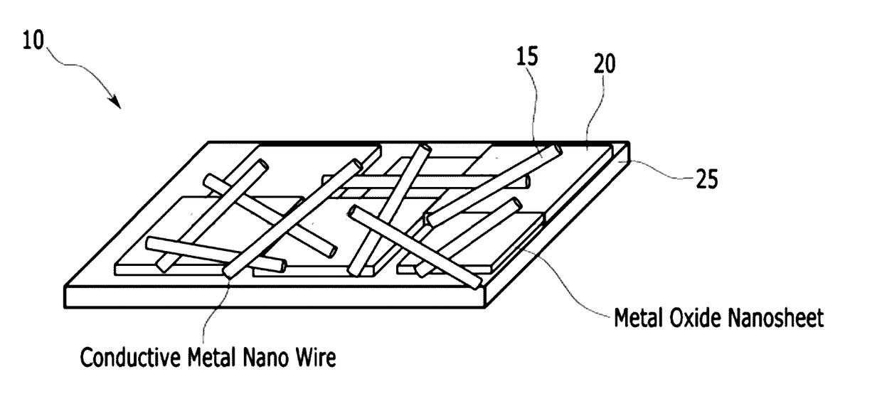
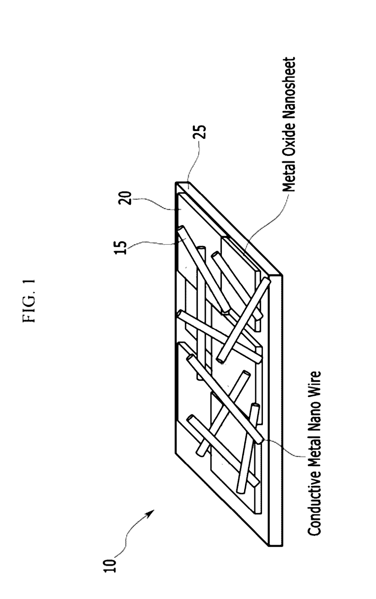
Electrical conductors, electrically conductive structures, and electronic devices including the same
a technology of electrical conductors and conductors, applied in the direction of non-conductive materials with dispersed conductive materials, conductive layers on insulating supports, inorganic chemistry, etc., can solve the problems of poor flexibility of ito and invariably cost more, and achieve enhanced transparency, enhanced conductivity, and improved nanowire-based conductors
- Summary
- Abstract
- Description
- Claims
- Application Information
AI Technical Summary
Benefits of technology
Problems solved by technology
Method used
Image

Examples
preparation example 1-1
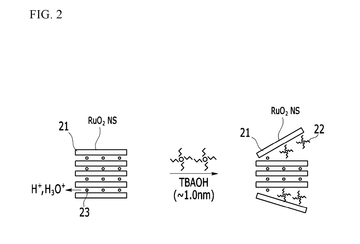
Preparation of Ruthenium Oxide Nanosheet via Exfoliation Using Two Types of Intercalants I
[0114]K2CO3 and RuO2 are mixed at a mole ratio of 5:8, and the mixture is pelletized. 4 grams (g) of the obtained pellet is introduced into an alumina crucible and heated in a tube furnace at 850 ° C. for 12 hours (h) under a nitrogen atmosphere. The total weight of the pellet may be changed within the range of 1 g to 100 g if desired. Then, the furnace is cooled to room temperature, and the treated pellet is taken out therefrom and ground to provide a fine powder.
[0115]The obtained fine powder is washed with 100 milliliters (mL) to 4 liters (L) of water for 24 h, and then filtered to provide a powder, the composition of which is K0.2RuO2.1.nH2O. The K0.2RuO2.1.nH2O powder is then introduced into a 1 molar (M) HCl solution and agitated for 3 days (d) and then filtered to provide a powder, the composition of which is H0.2RuO2.1.
[0116]1 g of the obtained H0.2RuO2.1 powder is introduced into 250 m...
preparation example 1-2
Preparation of Ruthenium Oxide Nanosheet via Exfoliation Using Two Types of Intercalants II
[0119]The RuO2.1 nanosheets are prepared in the same manner as set forth in Preparation Example 1-1 except that for exfoliation, 1g of the obtained H0.2RuO2.1 powder is introduced into 250 mL of an aqueous solution of TMAOH and TBAOH (the concentrations of TMAOH and TBAOH are TMA+ / H+=5 and TBA+ / H+=5, respectively) and agitated for 10 d or longer.
[0120]The SEM analysis is conducted for the exfoliated RuO2.1 nanosheets. Results of the SEM analysis confirm that the average lateral size of the nanosheets is 4.0 μm. An Atomic Force Microscope (AFM) is used to measure the thickness of the nanosheets, and the results confirm that the average thickness of the obtained nanosheets is about 1.23 nm.
preparation example 1-3
Preparation of Ruthenium Oxide Nanosheet via Exfoliation Using Two Types of Intercalants III
[0121]The RuO2.1 nanosheets are prepared in the same manner as set forth in Preparation Example 1-1 except that for exfoliation, 1 g of the obtained H0.2RuO2.1 powder is introduced into 250 mL of an aqueous solution of TMAOH and TBAOH (the concentrations of TMAOH and TBAOH are TMA+ / H+=5 and TBA+ / H+=5, respectively) and agitated for 3 days and then the resulting product is subjected to the ultrasonication for a predetermined time set forth in Table 3.
[0122]For the ultrasonication, a ultrasonic homogenisator (model name: UP400S Manufacturer: Hielscher) is used and the ultrasonic power is 80 W and the ultrasonication time is set for 1 minute to 60 minutes. The results are shown in Table 3:
[0123]The results are shown in Table 3:
TABLE 3Average lateral sizeof the nanosheetNanosheet con-Ultrasonicationand a standardcentration of thetimedeviation thereofcolloidal solution(min)(μm)(g / L)02.32 ± 1.810.8...
PUM
| Property | Measurement | Unit |
|---|---|---|
| Fraction | aaaaa | aaaaa |
| Thickness | aaaaa | aaaaa |
| Thickness | aaaaa | aaaaa |
Abstract
Description
Claims
Application Information
 - R&D
- Intellectual Property
- Life Sciences
- Materials
- Tech Scout
- Unparalleled Data Quality
- Higher Quality Content
- 60% Fewer Hallucinations
Browse by: Latest US Patents, China's latest patents, Technical Efficacy Thesaurus, Application Domain, Technology Topic, Popular Technical Reports.
© 2025 PatSnap. All rights reserved.Legal|Privacy policy|Modern Slavery Act Transparency Statement|Sitemap|About US| Contact US: help@patsnap.com