Carrier for mounting optical elements and associated fabrication process

a technology of optical elements and carriers, applied in the field of optical components, can solve the problems of not being able to scale well for mass production, not being able to meet the needs of mass production, and being costly and inconvenient to build optical links, etc., to achieve the effect of reducing cross-talk, reducing absorption and/or reflection losses, and increasing electrical design flexibility

Active Publication Date: 2017-04-13
TE CONNECTIVITY NEDERLAND
View PDF11 Cites 0 Cited by
  • Summary
  • Abstract
  • Description
  • Claims
  • Application Information

AI Technical Summary

Benefits of technology

[0008]Such an apparatus provides many important benefits including precision butt coupling an optical die to an optical fiber, having the optical axes of the die and fiber in line and obviating the need for a lens in between. A mounting pad arrangement is provided such that the optical axis of an optical die is mounted in-line with the axis of an optical fiber. Redirection of the light from the optical fiber is obviated and the die and fiber can be butt coupled without any optical components in between. This provides the advantage of eliminating absorption and / or reflection losses from optical components.
[0009]In addition to a mechanical function, the carrier part also provides electrical tracks and connection to the optical die without the requirement of introducing additional parts. The carrier part can also provide a bonding area for a driver or amplifier chip and in that way allows the electrical lines between the chip and optical die to be short, which is beneficial for signal integrity. Moreover, a multilayer carrier can also be used offering more electrical design flexibility, e.g., reducing cross-talk. Owing to the good thermal conductivity of the carrier, it serves as a heat-spreader, reducing the need to use expensive thermal bridges to the outside of the casing.

Problems solved by technology

Applicants recognize that typical approaches for building an optical link especially in the case of a printed circuit board are costly and inconvenient and may not scale well for mass production.

Method used


Image

  • Carrier for mounting optical elements and associated fabrication process
  • Carrier for mounting optical elements and associated fabrication process
  • Carrier for mounting optical elements and associated fabrication process

Examples


Embodiment Construction

Ablation Insusceptible and Ablation Susceptible Layers and Ablation Process

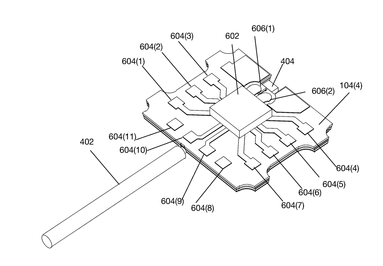
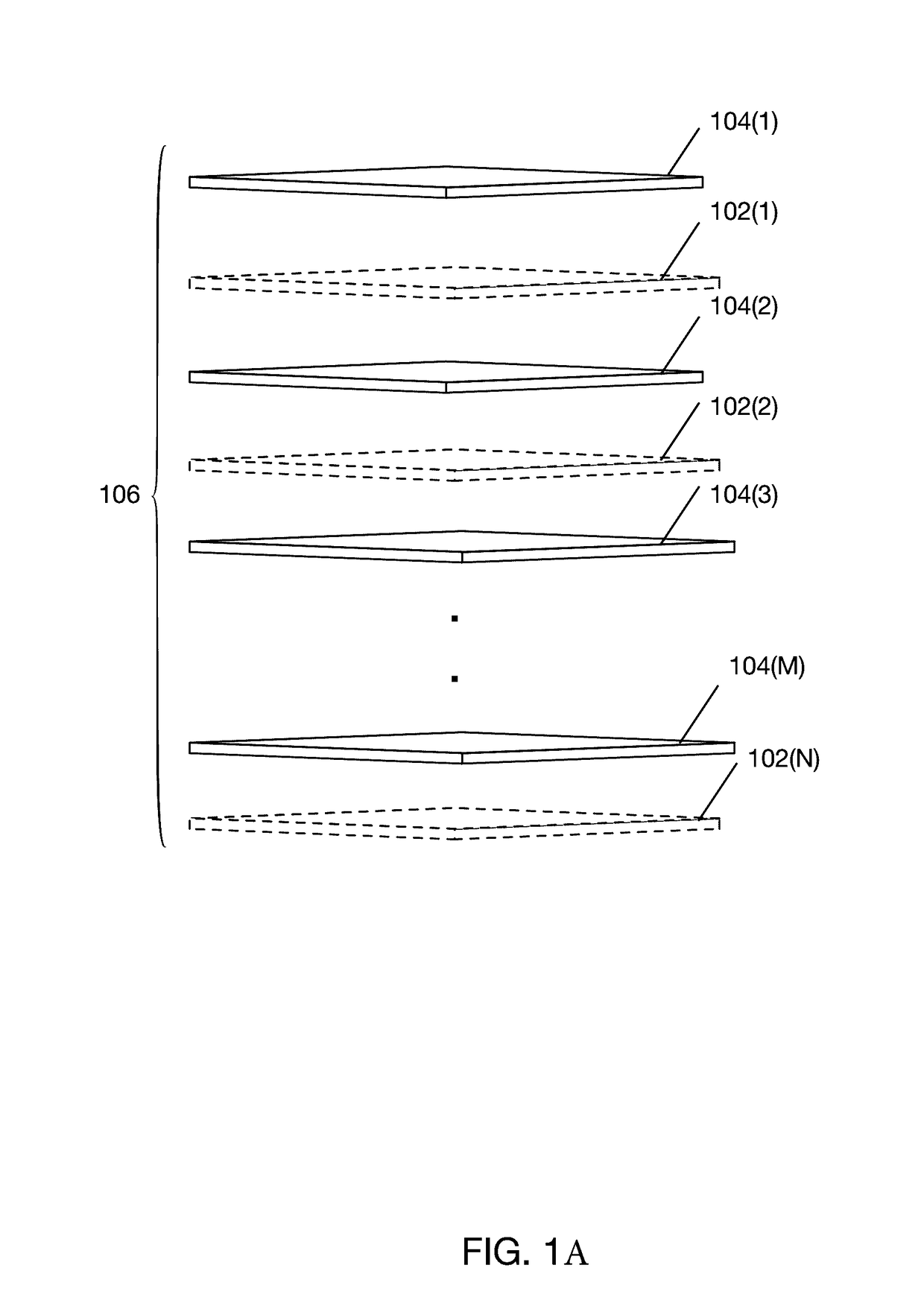
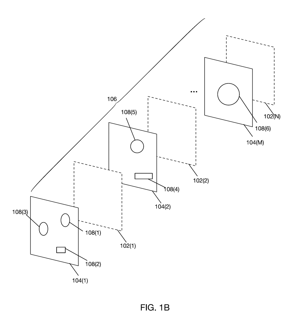
[0028]FIG. 1A shows a stack of alternating ablation susceptible and ablation insusceptible layers for generating an optical mounting structure according to one embodiment. Stack 106 comprises ablation insusceptible layers 104(1)-104(M) and ablation susceptible layers 102(1)-102(N). Ablation insusceptible layers 104(1)-104(M) each may exhibit a respective geometric pattern (not shown in FIG. 1A) and are insusceptible to erosion by an ablation process. According to one embodiment, layers 104(1)-104(M) may be comprised of copper. However, ablation insusceptible layers may be comprised of other materials including, for example, gold, nickel and other metals.

[0029]Ablation susceptible layers 102(1)-102(N) are susceptible to ablation by a laser process. According to one embodiment, ablation susceptible layers 102(1)-102(N) may be comprised of polyimide. However, ablation susceptible layers may be comprised of other...


PUM


Abstract

A low-cost and mass producible carrier part for precise mounting of optical components such as an optical fiber and optical die and associated fabrication process.

Description

FIELD OF INVENTION[0001]The invention relates generally to optoelectronics and a fabrication process for generating a carrier part allowing the precise mounting and alignment of optical elements.BACKGROUND[0002]Manufacturing a precision optical link between two optical components is typically complex and expensive. For example, the alignment of an optical fiber and an optical die (laser diode, photo diode) is crucial and requires significant precision.[0003]It is common industry practice to mount an optical die with its active layer (the plane of the wafer) parallel to a carrier such as a PCB or glass plate. The optical axis is then perpendicular to the surface of the carrier or circuit board. In many cases it is practical to orient the axis of the fiber parallel to the surface of the carrier or circuit board, in which case it becomes necessary to redirect the light by means of, for example, a mirror combined with a lens. Thus, conventional coupling schemes involve a perpendicular a...

Claims


Application Information

Patent Timeline
Patent Type & Authority Applications(United States)
IPC IPC(8): G02B6/42
CPCG02B6/4257G02B6/4295G02B6/423G02B6/4201G02B6/4245G02B6/4255G02B6/428G02B6/4296G02B6/4202G02B6/0083G02B6/009G02B5/223G02B6/43G02B6/136G02B2006/12173G02B2006/12176H01L23/49579H01L23/49822H01L23/49866
Inventor TUIN, JACOBUS NICOLAASDORRESTEIN, ALEXANDER JOHANNES ADRIANUS CORNELIADUIS, JEROEN ANTONIUS MARIASMINK, RUTGER WILHELMUSVAN RIJNBACH, MICHIEL
Owner TE CONNECTIVITY NEDERLAND
Why Eureka
Try Eureka