Generating high resolution images from low resolution images for semiconductor applications

a technology of low resolution images and semiconductors, applied in image enhancement, instruments, editing/combining figures or texts, etc., can solve the problems of general generation of image signals or data, time-consuming defect review and metrology, and time-consuming processes, and achieve high resolution images.

Active Publication Date: 2017-07-06
KLA TENCOR TECH CORP
View PDF3 Cites 140 Cited by
  • Summary
  • Abstract
  • Description
  • Claims
  • Application Information

AI Technical Summary

Problems solved by technology

However, as the dimensions of semiconductor devices decrease, inspection becomes even more important to the successful manufacture of acceptable semiconductor devices because smaller defects can cause the devices to fail.
As described above, therefore, due to the limited resolution with which inspection (optical and sometimes electron beam inspection) is performed, the specimen is generally needed to generate additional higher resolution images for defect review of the defects detected on the specimen, which may include verification of the detected defects, classification of the detected defects, and determining characteristics of the defects.
Therefore, defect review and metrology can be time consuming processes that require use of the physical specimen itself and additional tools (in addition to the inspector) needed to generate the higher resolution images.
Defect review and metrology, however, are not processes that can be simply eliminated to save time and money.
For example, due to the resolution with which inspection processes are performed, inspection processes do not in general generate image signals or data that can be used to determine information for the detected defects that is sufficient to classify the defects and / or determine a root cause of the defects.
In addition, due to the resolution with which inspection processes are performed, inspection processes do not in general generate image signals or data that can be used to determine information for patterned features formed on the specimen with sufficient accuracy.

Method used


Image

  • Generating high resolution images from low resolution images for semiconductor applications
  • Generating high resolution images from low resolution images for semiconductor applications
  • Generating high resolution images from low resolution images for semiconductor applications

Examples


Embodiment Construction

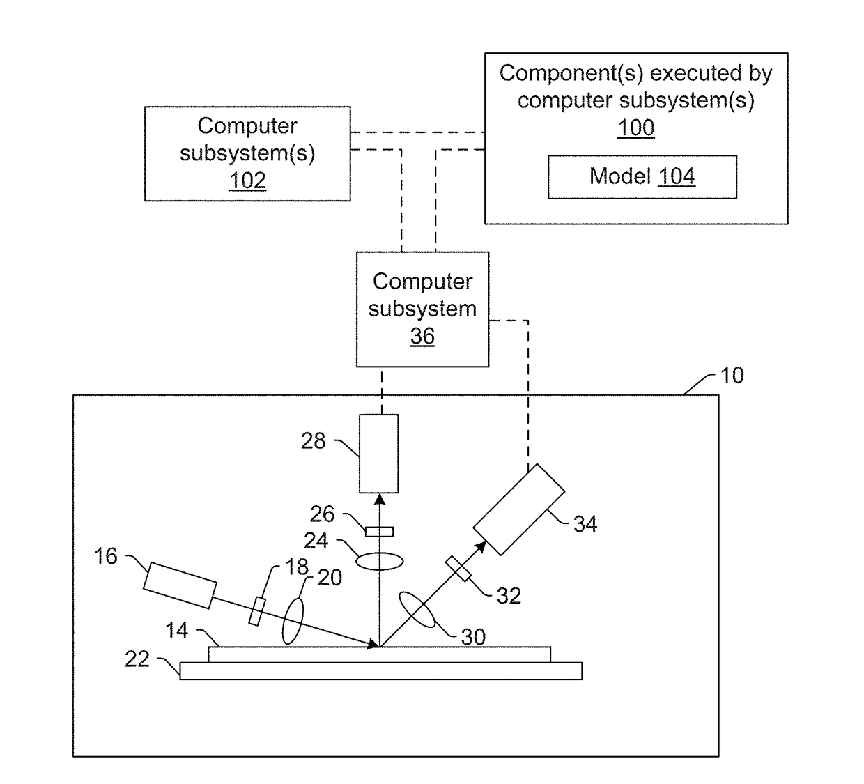
[0026]The tennis “design,”“design data,” and “design information” as used interchangeably herein generally refer to the physical design (layout) of an IC and data derived from the physical design through complex simulation or simple geometric and Boolean operations. In addition, an image of a reticle acquired by a reticle inspection system and / or derivatives thereof can be used as a “proxy” or “proxies” for the design. Such a reticle image or a derivative thereof can serve as a substitute for the design layout in any embodiments described herein that use a design. The design may include any other design data or design data proxies described in commonly owned U.S. Pat. Nos. 7,570,796 issued on Aug. 4, 2009 to Zafar et al. and 7,676,077 issued on Mar. 9, 2010 to Kulkarni et al., both of which are incorporated by reference as if fully set forth herein. In addition, the design data can be standard cell library data, integrated layout data, design data for one or more layers, derivatives...


PUM

PropertyMeasurementUnit
high resolution imagingaaaaaaaaaa
high magnification optical systemaaaaaaaaaa
scanning electron microscopeaaaaaaaaaa

Abstract

Methods and systems for generating a high resolution image for a specimen from one or more low resolution images of the specimen are provided. One system includes one or more computer subsystems configured for acquiring one or more low resolution images of a specimen. The system also includes one or more components executed by the one or more computer subsystems. The one or more components include a model that includes one or more first layers configured for generating a representation of the one or more low resolution images. The model also includes one or more second layers configured for generating a high resolution image of the specimen from the representation of the one or more low resolution images.

Description

BACKGROUND OF THE INVENTION[0001]1. Field of the Invention[0002]The present invention generally relates to methods and systems for generating high resolution images from low resolution images for semiconductor applications.[0003]2. Description of the Related Art[0004]The following description and examples are not admitted to be prior art by virtue of their inclusion in this section.[0005]Fabricating semiconductor devices such as logic and memory devices typically includes processing a substrate such as a semiconductor wafer using a large number of semiconductor fabrication processes to form various features and multiple levels of the semiconductor devices. For example, lithography is a semiconductor fabrication process that involves transferring a pattern from a reticle to a resist arranged on a semiconductor wafer. Additional examples of semiconductor fabrication processes include, but are not limited to, chemical-mechanical polishing (CMP), etch, deposition, and ion implantation. ...

Claims


Application Information

Patent Timeline
Patent Type & Authority Applications(United States)
IPC IPC(8): G06T11/60H01L21/67G01N21/95G06K9/62G06T7/00
CPCG06T11/60G06K9/6269G06T7/0004G01N2201/12H01L21/67288G06T2207/30148G01N21/9501G06T3/4053G06V10/454G06V30/2504G06V2201/06G06V10/82G06V30/19173G06T3/4076G06F18/2414
Inventor ZHANG, JINGCHEN, GRACE HSIU-LINGBHASKAR, KRISWELLS, KEITHBAI, NANGU, PINGGAO, LISHENG
Owner KLA TENCOR TECH CORP
Why Eureka
Try Eureka