Method for implantation of semiconductor wafers having high bulk resistivity

a technology of bulk resistivity and semiconductor wafers, which is applied in the direction of semiconductor/solid-state device testing/measurement, electrical equipment, electric discharge tubes, etc., can solve the problems of affecting the stability of hbr wafer monitoring, affecting the processing of hbr wafers in ion implanters, and affecting the processing efficiency of hbr wafers, etc., to achieve high bulk resistivity

Active Publication Date: 2017-07-20
VARIAN SEMICON EQUIP ASSOC INC
View PDF0 Cites 12 Cited by
  • Summary
  • Abstract
  • Description
  • Claims
  • Application Information

AI Technical Summary

Benefits of technology

[0008]In one embodiment, an ion implanter may include an electrostatic clamp to hold a substrate; a plasma flood gun generating a flux of electrons impinging upon the substrate; and a controller coupled to the plasma flood gun and including a component generating a control signal responsive to a measurement signal, the control signal to adjust operation of the plasma flood gun to a target operating level. At the target operating level the flux of electrons may comprise a stabilizing dose of electrons, the stabilizing concentration of electrons, the stabilizing concentration reducing a clamp current variation in the electrostatic clamp to a target value, the target value being less than a second value of clamp current variation when the plasma flood gun is not operating.
[0009]In another embodiment, a method may include implanting a high bulk resistivity (HBR) wafer, the HBR wafer having

Problems solved by technology

One issue encountered when implanting HBR substrates such as semiconductor wafers having resistivity above 10-30 Ω-cm is the ability to process the HBR semiconductor wafers (“HBR wafers”) without encountering handling errors during an implantation process, including processing in high current or medium current ion implantation apparatus.
This method may work adequately for substrates having a resistivity of 10-30 Ω-cm, but may not work well for HBR substrates, leading to wafer handling problems.
Because HBR wafers may engender such instabilities, the pro

Method used


Image

  • Method for implantation of semiconductor wafers having high bulk resistivity
  • Method for implantation of semiconductor wafers having high bulk resistivity
  • Method for implantation of semiconductor wafers having high bulk resistivity

Examples


Embodiment Construction

[0021]For the sake of convenience and clarity, terms such as “top,”“bottom,”“upper,”“lower,”“vertical,”“horizontal,”“lateral,” and “longitudinal” will be used herein to describe the relative placement and orientation of these components and their constituent parts with respect to the geometry and orientation of a component of a device as appearing in the figures. The terminology will include the words specifically mentioned, derivatives thereof, and words of similar meaning and / or significance.

[0022]As used herein, an element or operation recited in the singular and proceeded with the word “a” or “an” is to be understood as including plural elements or operations, until such exclusion is explicitly recited. Furthermore, references to “one embodiment” of the present disclosure are not intended as limiting. Additional embodiments may also incorporate the recited features.

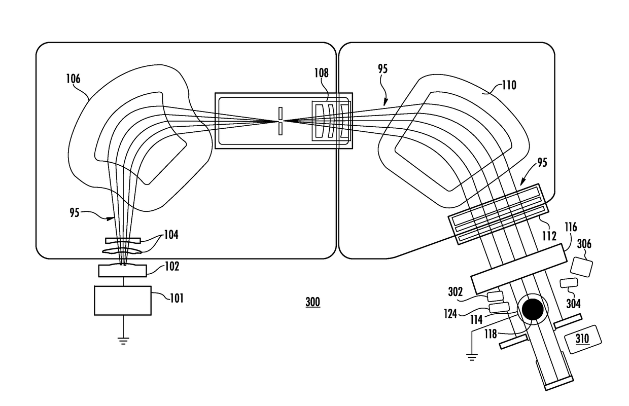
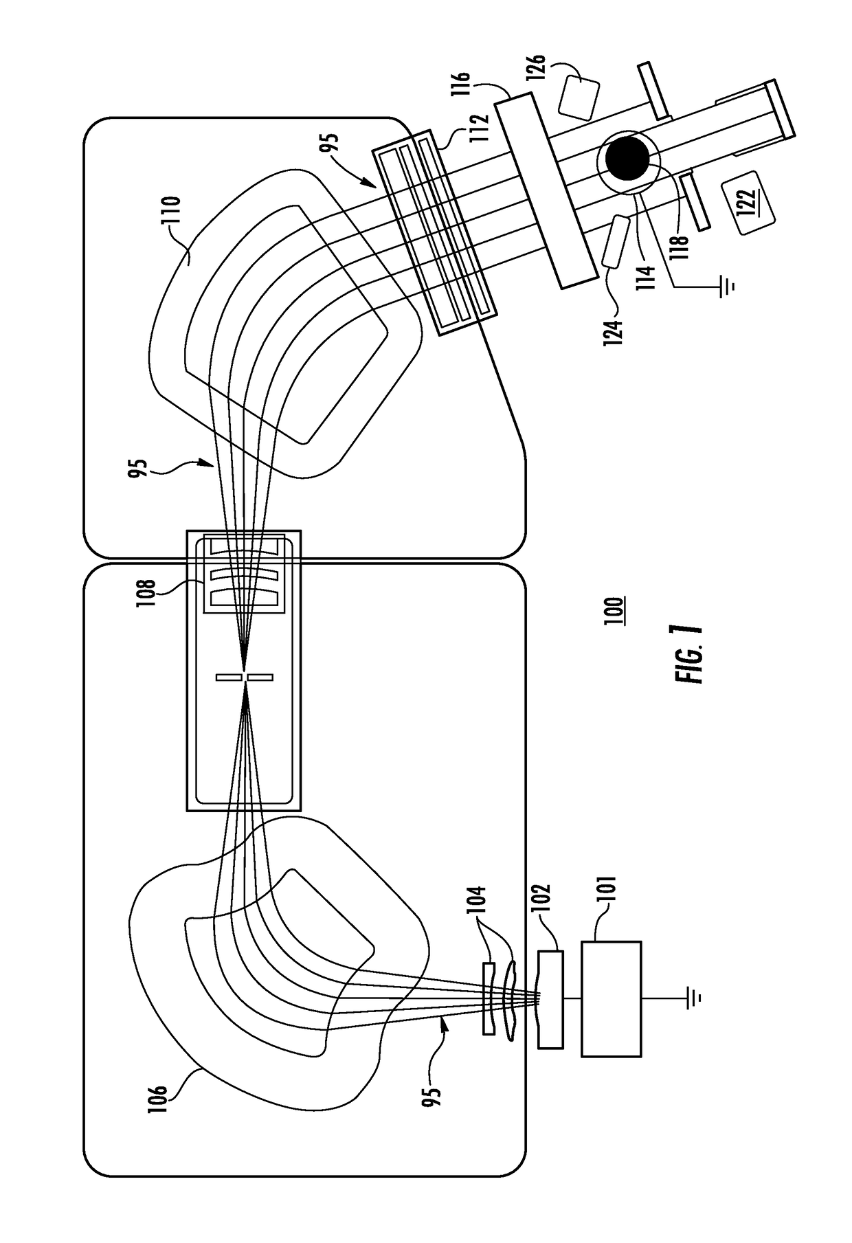
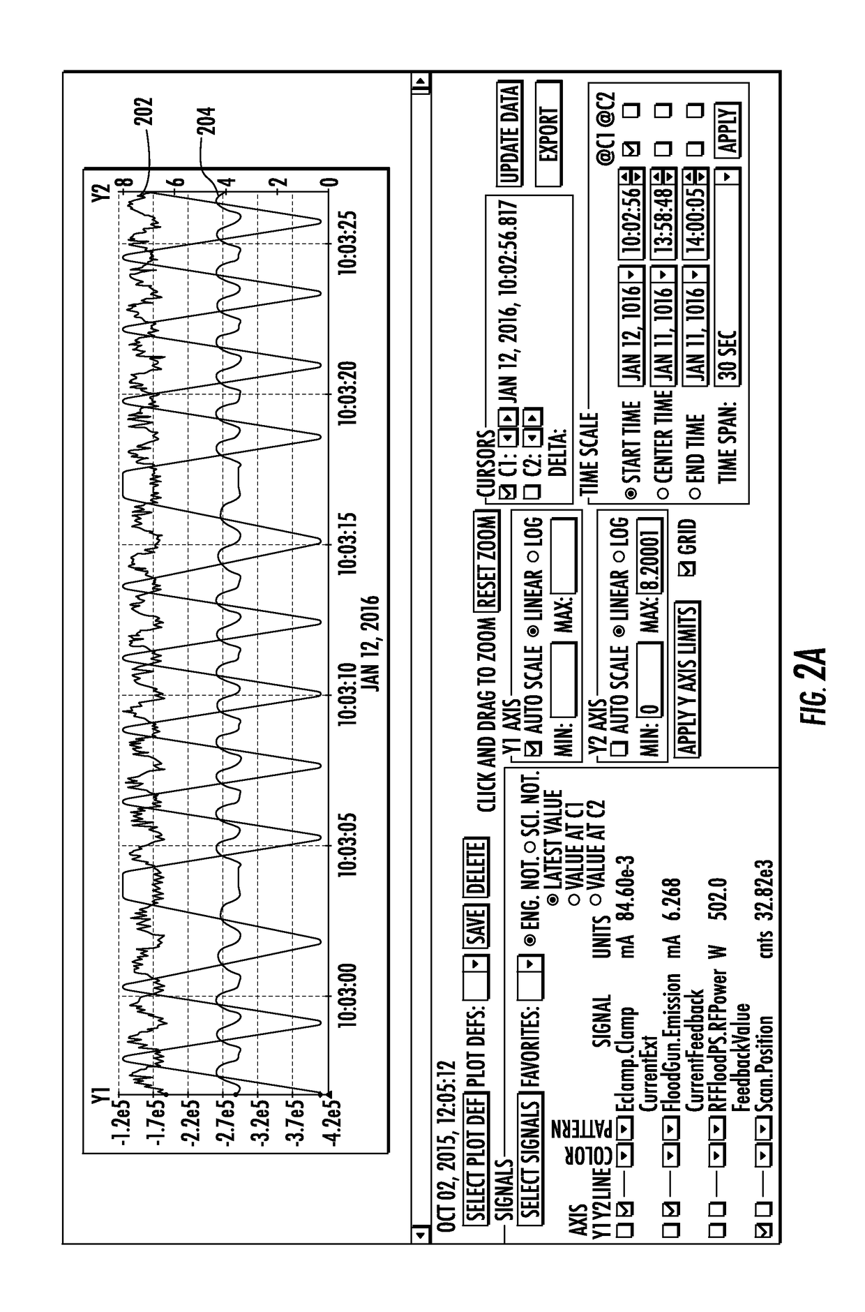
[0023]Various embodiments of the disclosure provide apparatus, systems, and methods for improved substrate processi...


PUM


Abstract

An ion implanter may include an electrostatic clamp to hold a substrate; a plasma flood gun generating a flux of electrons impinging upon the substrate; and a controller coupled to the plasma flood gun and including a component generating a control signal responsive to a measurement signal, the control signal to adjust operation of the plasma flood gun to a target operating level. At the target operating level the flux of electrons may comprise a stabilizing dose of electrons, the stabilizing concentration of electrons, the stabilizing concentration reducing a clamp current variation in the electrostatic clamp to a target value, the target value being less than a second value of clamp current variation when the plasma flood gun is not operating.

Description

RELATED APPLICATIONS[0001]This application claims priority to U.S. provisional patent application No. 62 / 278,950 filed Jan. 14, 2016 and incorporated by reference herein in its entirety.FIELD OF THE DISCLOSURE[0002]Embodiments of the disclosure relate generally to techniques for manufacturing devices, and more particularly, to techniques for improved processing of substrates in an ion implantation apparatus.BACKGROUND OF THE DISCLOSURE[0003]Ion implantation is a process for introducing of introducing dopants, additives, or impurities into a substrate via ion bombardment. Known ion implantation systems or apparatus may comprise an ion source and a series of beam-line components. The ion source may comprise a chamber where desired ions are generated. The ion source may also comprise a power source and an extraction electrode assembly disposed near the chamber. The beam-line components, may include, for example, a mass analyzer, a first acceleration or deceleration stage, a collimator,...

Claims


Application Information

Patent Timeline
IPC IPC(8): H01J37/304H01L21/66H01J37/317H01L21/265
CPCH01J37/304H01L21/265H01L22/14H01J2237/30405H01J37/3171H01J2237/31703H01L22/20H01J37/026H01J37/20H01J2237/2007H01J27/02H01J37/30H01J37/317H01L21/26586H01L21/425H01L21/67213
Inventor OSBORNE, MICHAEL W.SUURONEN, DAVID E.BLAKE, JULIAN G.
Owner VARIAN SEMICON EQUIP ASSOC INC
Why Eureka
Try Eureka