Piezoelectric element, piezoelectric element application device, and method of manufacturing piezoelectric element

a piezoelectric element and piezoelectric technology, applied in the direction of piezoelectric/electrostrictive/magnetostrictive devices, printing, electrical apparatus, etc., can solve the problems of difficult to homogenize the composition distribution (k:na) at the microscopic level, difficult to make the composition in the in-plane direction homogeneous,

Active Publication Date: 2017-08-10
SEIKO EPSON CORP
View PDF2 Cites 20 Cited by
  • Summary
  • Abstract
  • Description
  • Claims
  • Application Information

AI Technical Summary

Benefits of technology

[0009]An advantage of some aspects of the present invention is to provide a piezoelectric element which has a KNN layer formed by a wet method which is a piezoelectric layer with a homogeneous composition distribution in the in-plane direction and the film thickness direction, a piezoelectric element application device, and a method of manufacturing a piezoelectric element.

Problems solved by technology

Since a KNN sintered body produced by a sintering method is the target in the sputtering method, it is difficult to homogenize the composition distribution (K:Na) at the microscopic level.
In addition, taking into account that non-homogeneity of the composition distribution at the microscopic level extends in the in-plane direction, it is considered that the KNN layer formed by this method has a homogeneous composition in the film thickness direction, but that it is difficult to make the composition in the in-plane direction homogeneous.
However, in the wet method, since the KNN layer is formed by stacking the KNN thin film, there is a composition distribution (K:Na) in the film thickness direction (it is difficult to make the composition homogeneous).
Here, this problem is not only limited to piezoelectric elements used in piezoelectric actuators mounted in a liquid ejecting head which is represented by an ink jet recording head, but this problem also similarly affects piezoelectric elements used in other piezoelectric element application devices.

Method used


Image

  • Piezoelectric element, piezoelectric element application device, and method of manufacturing piezoelectric element
  • Piezoelectric element, piezoelectric element application device, and method of manufacturing piezoelectric element
  • Piezoelectric element, piezoelectric element application device, and method of manufacturing piezoelectric element

Examples


embodiment 1

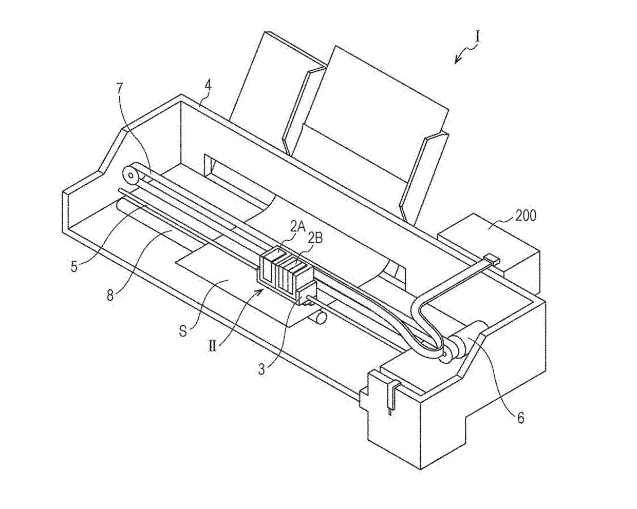
[0041]FIG. 1 is an ink jet recording apparatus which is an example of a liquid ejecting apparatus provided with a recording head which is an example of a piezoelectric element application device. As shown in the diagram, in the ink jet recording apparatus (recording apparatus) I, cartridges 2A and 2B, which form the ink supply means, are detachably attached as the ink jet recording head unit (head unit) II which has a plurality of ink jet recording heads. The carriage 3 on which the head unit II is mounted is provided to be freely movable, in the axial direction, on a carriage shaft 5 attached to the apparatus main body 4 and, for example, ejects each color ink composition and a black ink composition.

[0042]Here, by transmitting the driving force of the driving motor 6 to the carriage 3 via a plurality of gears (not shown) and the timing belt 7, the carriage 3 on which the head unit II is mounted is moved along the carriage shaft 5. On the other hand, a transport roller 8 is provided...

example 1

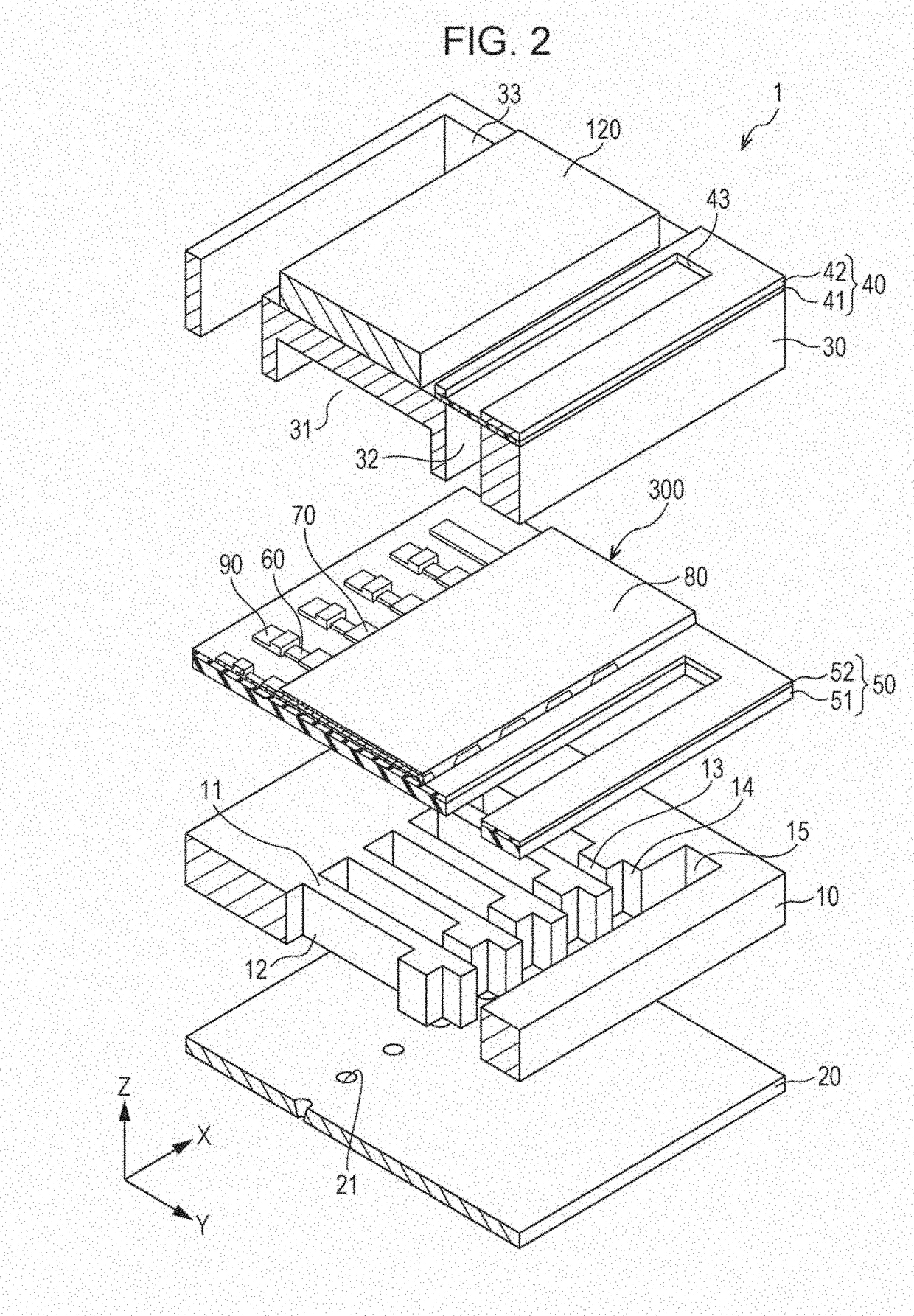
[0105]By thermal oxidation of the surface of the silicon substrate which is the substrate 10, the elastic film 51 formed of silicon dioxide was formed on the silicon substrate. Next, by forming a zirconium film by a sputtering method on the elastic film 51 and carrying out thermal oxidation on the zirconium film, the insulating film 52 formed of zirconium oxide was formed. Next, by forming a titanium film by a sputtering method on the insulating film 52 and carrying out thermal oxidation on the titanium film, an adhesive layer 56 formed of titanium oxide was formed. Then, after forming a platinum film by a sputtering method on the adhesive layer 56, by pattering into a predetermined shape, the first electrodes 60 with a thickness of 50 nm were formed.

[0106]Next, the piezoelectric layer 70 was formed by the following procedure. First, a 2-n-butoxyethanol solution of potassium acetate, an n-octane solution of sodium acetate, and a 2-n-ethylhexanoic acid solution of pentaethoxyniobium ...

example 2

[0109]The piezoelectric layer 70 of Example 2 was formed in the same manner as Example 1 except that the first piezoelectric film 71 with a thickness of 35 nm was formed, and the piezoelectric layer 70 with a thickness of 515 nm formed of seven layers of piezoelectric films was formed.


PUM


Abstract

A piezoelectric element includes a first electrode, a piezoelectric layer formed of a first piezoelectric film which is formed on the first electrode and which includes potassium, sodium, and niobium and a plurality of second piezoelectric films which are formed on the first piezoelectric film and which include potassium, sodium, and niobium, and a second electrode formed on the piezoelectric layer, in which the piezoelectric layer is a stack of a plurality of piezoelectric films, the first piezoelectric film has a thickness of 30 nm to 70 nm, a concentration of sodium in each of the piezoelectric films is along a gradient in the film thickness direction with the first electrode side being high and the second electrode side being low.

Description

BACKGROUND[0001]1. Technical Field[0002]The present invention relates to a piezoelectric element, a piezoelectric element application device which is provided with a piezoelectric element, and a method of manufacturing a piezoelectric element.[0003]2. Related Art[0004]In general, piezoelectric elements have a piezoelectric layer which has electro-mechanical conversion characteristics, and two electrodes with the piezoelectric layer interposed therebetween. In recent years, devices (piezoelectric element application devices) using such piezoelectric elements as a driving source have been actively developed. As a piezoelectric element application device, there are liquid ejecting heads which are represented by an ink jet recording head, MEMS elements which are represented by a piezoelectric MEMS element, ultrasonic measuring apparatuses which are represented by an ultrasonic sensor or the like, as well as piezoelectric actuator apparatuses, and the like.[0005]As a material (piezoelect...

Claims


Application Information

Patent Timeline
Patent Type & Authority Applications(United States)
IPC IPC(8): H01L41/27B41J2/14H01L41/047H01L41/187H01L41/083
CPCH01L41/27H01L41/1873B41J2/14274H01L41/0472H01L41/083B41J2/14233B41J2002/14258B41J2/161B41J2/1623B41J2/1628B41J2/1629B41J2/1635B41J2/1646B41J2002/14241B41J2002/14419B41J2202/03H10N30/1051H10N30/8542H10N30/078H10N30/05H10N30/50H10N30/872
Inventor SAKAI, TOMOHIROKITADA, KAZUYASUMI, KOJI
Owner SEIKO EPSON CORP
Why Eureka
Try Eureka