
Polycrystalline silicon and method for selecting polycrystalline silicon

Inactive Publication Date: 2017-08-17
SHIN ETSU CHEM IND CO LTD
View PDF5 Cites 0 Cited by
  • Summary
  • Abstract
  • Description
  • Claims
  • Application Information

AI Technical Summary

Benefits of technology

The patent text explains that the size of the grains in polycrystalline silicon is important for producing high-quality single crystal silicon. The text provides a simple method to select suitable polycrystalline silicon for this purpose. The technical effect of this invention is to ensure a high yield of high-quality single crystal silicon.

Problems solved by technology

Therefore, some unmelted crystallites pass, in the form of a solid particle, through a melting zone into a single crystal rod to be formed, and are incorporated into a solidified surface of the single crystal, resulting in causing defect formation.
In the visual determination under an optical microscope as in the method disclosed in Japanese Patent Laid-Open No. 2008-285403, however, a difference can be easily caused in the result depending on the degree of the etching of a sample surface to be observed or the observation skill and the like of an evaluator, and in addition, this method is poor in quantitativeness and reproducibility.
Therefore, from the viewpoint of increasing the production yield of single crystal silicon, it is necessary to set a rather high criterion for quality determination of polycrystalline silicon used as a raw material, and hence, a rejection rate of polycrystalline silicon rods is unavoidably increased.
Besides, according to the study made by the present inventors, when the method disclosed in Japanese Patent Laid-Open No. 2008-285403 is employed, even if a polycrystalline silicon rod determined as good is used, dislocation may be caused during the growth of a single crystal silicon rod by the FZ method to cause a crystal line to disappear in some cases.

Method used


Image

  • Polycrystalline silicon and method for selecting polycrystalline silicon
  • Polycrystalline silicon and method for selecting polycrystalline silicon

Examples


examples

[0030]Now, examples of the application of the present invention to a polycrystalline silicon rod synthesized by the Siemens process will be described. A core sample with a diameter of 19 mm (having a length of 130 mm) was collected from each polycrystalline silicon rod, produced by the Siemens process, in a direction vertical to the lengthwise direction (vertical direction). Besides, three core samples each with the same diameter (having a length of 130 mm) were similarly collected, in a direction parallel to the lengthwise direction, respectively from a region close to the core, a region corresponding to a half of the radius (R / 2) of the polycrystalline silicon rod, and a region close to the outer surface thereof. Incidentally, four polycrystalline silicon rods A, B, C and D were prepared for the examples, and it is noted that these rods were obtained by separating polycrystalline silicon under different conditions.

[0031]From each of these core samples, plate-shaped samples each ha...


PUM


Abstract

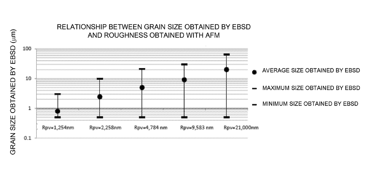
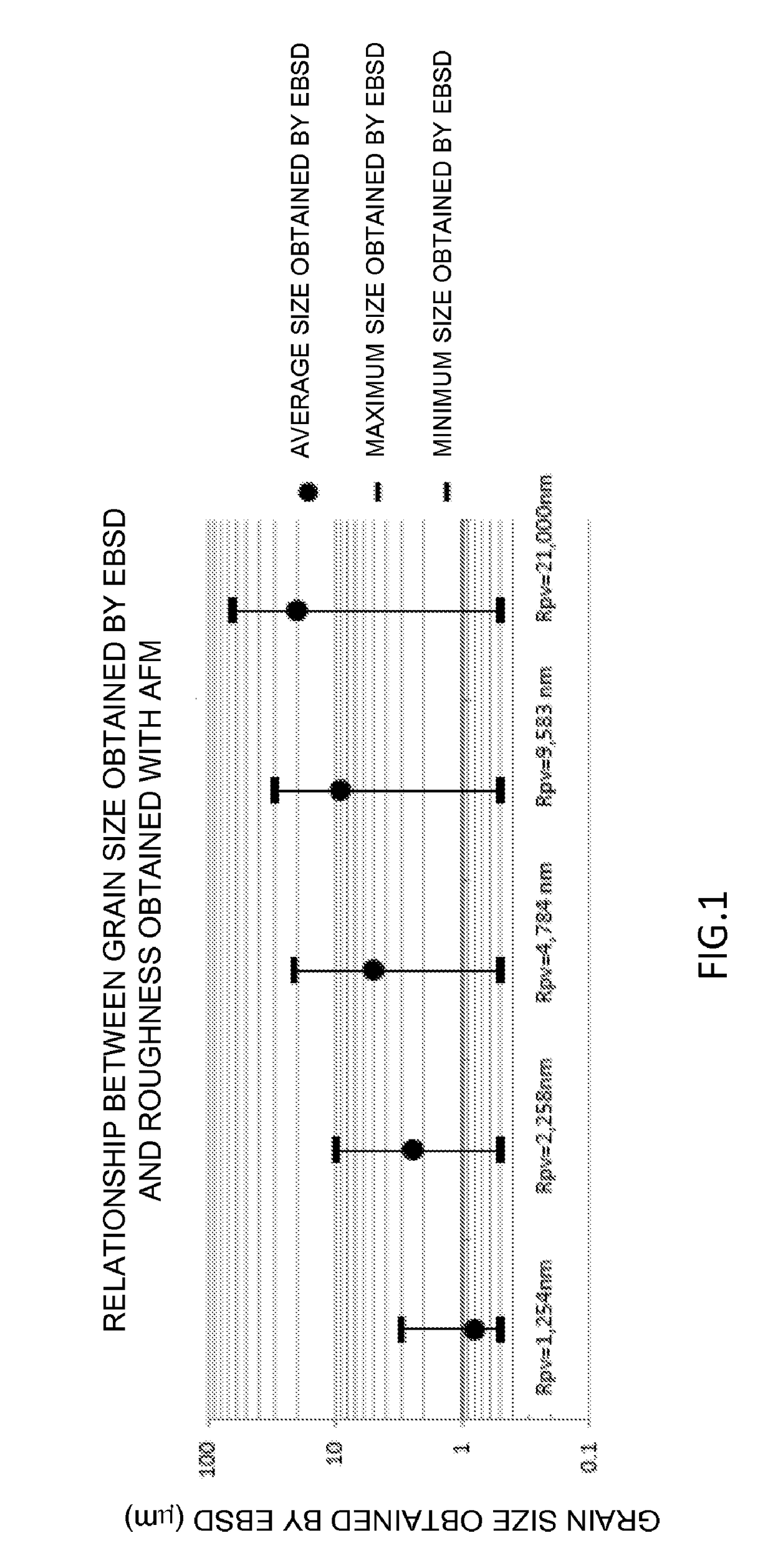
An object of the present invention is to provide a method for comparatively simply selecting polycrystalline silicon suitably used for stably producing single crystal silicon in high yield. According to the present invention, polycrystalline silicon having a maximum surface roughness (Peak-to-Valley) value Rpv of 5000 nm or less, an arithmetic average roughness value Ra of 600 nm or less and a root mean square roughness value Rq of 600 nm or less, the surface roughness values being measured by observing with an atomic force microscope (AFM) the surface of a collected plate-shaped sample, is selected as a raw material for producing single crystal silicon.

Description

BACKGROUND OF THE INVENTIONField of the Invention[0001]The present invention relates to a technique for producing polycrystalline silicon, and more particularly, it relates to a technique for evaluating polycrystalline silicon suitably used for stable production of single crystal silicon.Description of the Related Art[0002]Single crystal silicon indispensable for production of semiconductor devices and the like is obtained through crystal growth by a CZ method or an FZ method, and a polycrystalline silicon rod or a polycrystalline silicon mass is used as a raw material in the production. In many cases, such a polycrystalline silicon material is produced by the Siemens process. In the Siemens process, a silane material gas such as trichlorosilane or monosilane is brought into contact with a heated silicon core wire, so as to vapor phase deposit (separate) polycrystalline silicon on the surface of the silicon core wire by CVD (Chemical Vapor Deposition), and thus, polycrystalline sili...

Claims


Application Information

Patent Timeline
IPC IPC(8): G01B21/30G01Q30/20C30B29/06C01B33/02C30B13/00C30B15/00
CPCG01B21/30C30B13/00C30B15/00C01P2006/90C01B33/02G01Q30/20C30B29/06C30B33/10C01B33/035H01L21/76254C01P2004/04C30B35/007B07B13/003
Inventor MIYAO, SHUICHINETSU, SHIGEYOSHI
Owner SHIN ETSU CHEM IND CO LTD
Learn More