Check patentability & draft patents in minutes with Patsnap Eureka AI!

Multi-channel integrated optical wavelength division multiplexing/demultiplexing assembly structure

Inactive Publication Date: 2017-08-24
WUHAN TELECOMM DEVICES
View PDF14 Cites 9 Cited by
  • Summary
  • Abstract
  • Description
  • Claims
  • Application Information

AI Technical Summary

Benefits of technology

The present invention uses an optical chip to improve the size and mounting accuracy of light assemblies made with multiple channels. This improves the product yield and increases production efficiency, reducing costs.

Problems solved by technology

At present, the rate of semiconductor lasers is limited by the bottlenecks of semiconductor and photoelectricity technology, and the rate of single-channel commercial products cannot be increased for the moment.
In addition, the offset in the degree of parallelism and the spacing of the multiple channels of collimated lights will also make the light beams from all the channels unable to be overlapped well finally.
In conclusion, the conventional light transmitting / receiving assembly structure with a multi-channel integrated optical wavelength division multiplexing / demultiplexing function has very strict requirements on the machining tolerance of the related materials and the mounting accuracy, and consequently, the material cost and the production cost are increased greatly.

Method used


Image

  • Multi-channel integrated optical wavelength division multiplexing/demultiplexing assembly structure
  • Multi-channel integrated optical wavelength division multiplexing/demultiplexing assembly structure
  • Multi-channel integrated optical wavelength division multiplexing/demultiplexing assembly structure

Examples


Embodiment Construction

[0031]The present invention will be further described below with reference to the accompanying drawings.

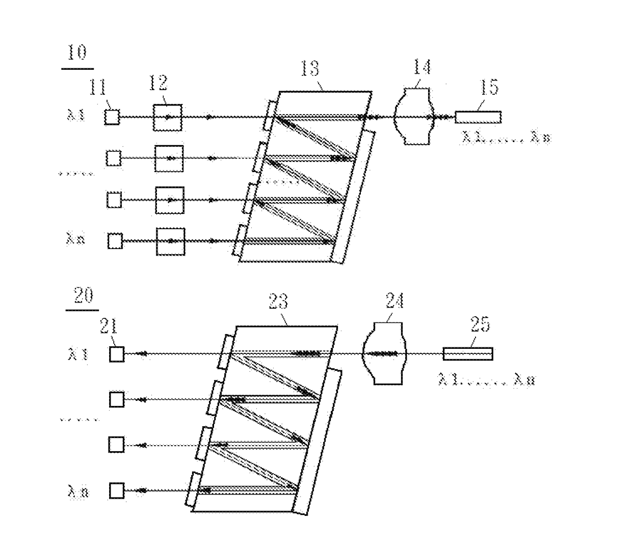
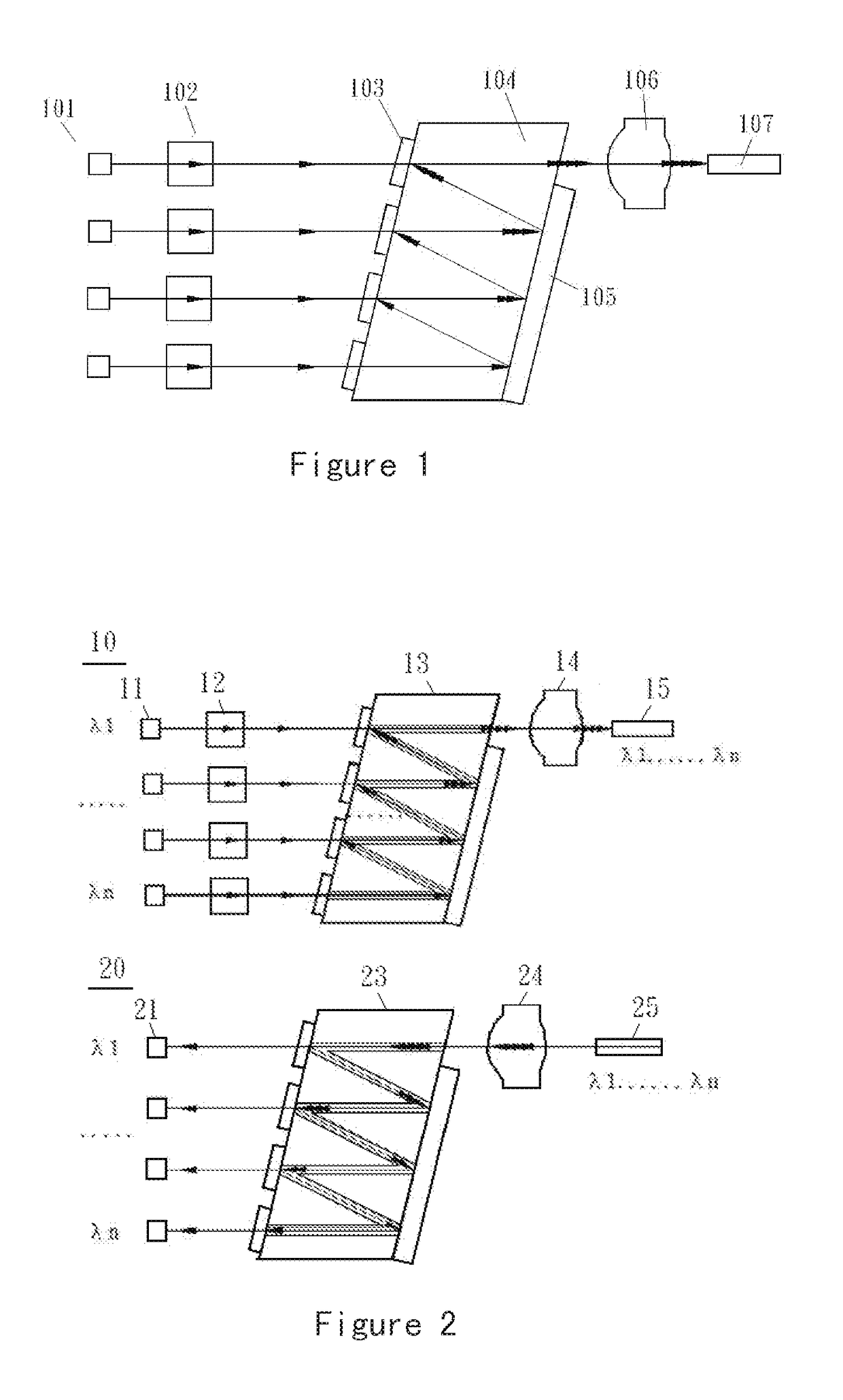
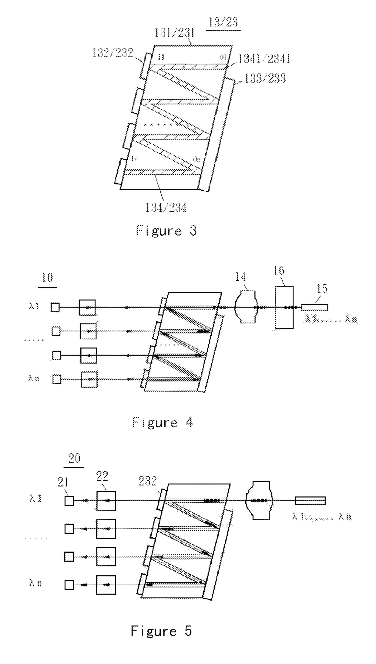
[0032]With reference to FIG. 2, the present invention provides a multi-channel integrated optical wavelength division multiplexing / demultiplexing assembly structure, comprising a light transmitting assembly 10 and a light receiving assembly 20.

[0033]In that, the light transmitting assembly 10 consists of a laser chip array 11, a coupling lens set 12, a wavelength division multiplexing assembly 13, a single coupling lens 14 and a single-core optical fiber 15, wherein the laser chip array 11 may be an array formed by a plurality of discrete laser chips of different wavelengths or a laser chip array having a plurality of light emitting units of different wavelengths; the wavelengths of the channels may be different CWDM, LWDM or DWDM wavelengths meeting the IEEE specifications, or may be any other wavelengths; and, the number n of the array channels may be 4, 6 or any other number. O...


PUM


Abstract

The present invention provides a multi-channel integrated optical wavelength division multiplexing / demultiplexing assembly structure, comprising a light transmitting assembly and a light receiving assembly, the light transmitting assembly consisting of a laser chip array, a coupling lens set, a wavelength division multiplexing assembly, a single coupling lens and a single-core optical fiber, wherein the wavelength division multiplexing assembly comprises an optical waveguide chip, a band-pass filter set, a full-wavelength reflection unit, and multiple segments of waveguide optical paths that are continuously distributed in the optical waveguide chip in a Z-shape or W-shape, each of the multiple segments of waveguide optical paths has an input port and an output port which are distributed on left and right sides of the optical waveguide chip, respectively, the output ports comprise a tail end port which is arranged in correspondence to the single coupling lens, the band-pass filter set covers the input ports, and the full-wavelength reflection unit covers the output ports other than the tail end port. With the combination of the foregoing structure configurations, the technical problem of the presence of accuracy offset of the overall optical path is solved, and the effects of easy assembly, reduced cost and improved product yield are realized.

Description

TECHNICAL FIELD[0001]The present invention relates to the technical field of optical communication, and in particular to a multi-channel integrated optical wavelength division multiplexing / demultiplexing assembly structure.BACKGROUND OF THE PRESENT INVENTION[0002]With the rapid growth of the demand of modern communication on bandwidth, the requirements proposed by optical communication systems on high-speed optical transceiver module and on the light transmitting assemblies and the light receiving assemblies in the module are enhanced increasingly. The following main development trends are shown: higher rate, smaller size of the optical transceiver modules and lower power consumption.[0003]At present, the rate of semiconductor lasers is limited by the bottlenecks of semiconductor and photoelectricity technology, and the rate of single-channel commercial products cannot be increased for the moment. In order to improve the transmission capacity of optical communication equipments per ...

Claims


Application Information

Patent Timeline
IPC IPC(8): G02B6/293G02B6/12G02B6/30G02B6/32
CPCG02B6/29367G02B6/2938G02B6/30G02B6/12007G02B6/32G02B6/4206G02B6/4215G02B2006/12109H04J14/02
Inventor LIN, XUEFENGHU, BAIQUANLIU, CHENGGANGYU, XIANGHONG
Owner WUHAN TELECOMM DEVICES
Features
  • R&D
  • Intellectual Property
  • Life Sciences
  • Materials
  • Tech Scout
  • Unparalleled Data Quality
  • Higher Quality Content
  • 60% Fewer Hallucinations
Learn More