
High aspect ratio contact metallization without seams

a contact metallization and high aspect ratio technology, applied in the field of electrical, electronic and computer arts, can solve the problems of forming vertical seams within the metal contact, not meeting the resistance targets required, and the current metallization techniques are not able to deliver structures that meet the resistance targets

Active Publication Date: 2017-09-28
IBM CORP
View PDF2 Cites 5 Cited by
  • Summary
  • Abstract
  • Description
  • Claims
  • Application Information

AI Technical Summary

Benefits of technology

This patent text describes a new technique for creating high-speed semiconductor devices. This technique allows for the creation of structures with low resistance and seamless metal contact structures. Existing metal deposition processes are compatible with this technique, making it easy to integrate into existing manufacturing processes. Overall, this technique offers a faster and more efficient way to create better semiconductor devices.

Problems solved by technology

As the dimensions of tungsten metal contacts are scaled down for future technology nodes, currently used metallization techniques may not be able to deliver structures that meet the resistance targets required.
The process of filling high aspect ratio contact holes using conformal deposition processes often results in the formation of vertical seams within the metal contacts.

Method used


Image

  • High aspect ratio contact metallization without seams
  • High aspect ratio contact metallization without seams
  • High aspect ratio contact metallization without seams

Examples


Embodiment Construction

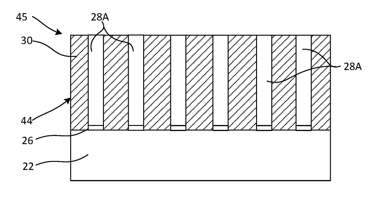
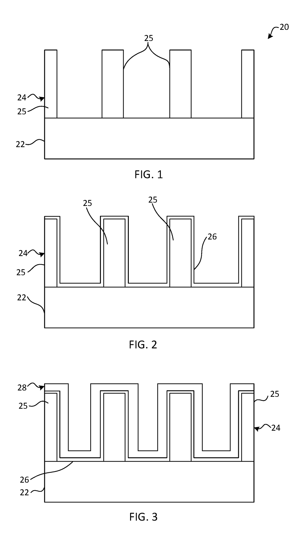
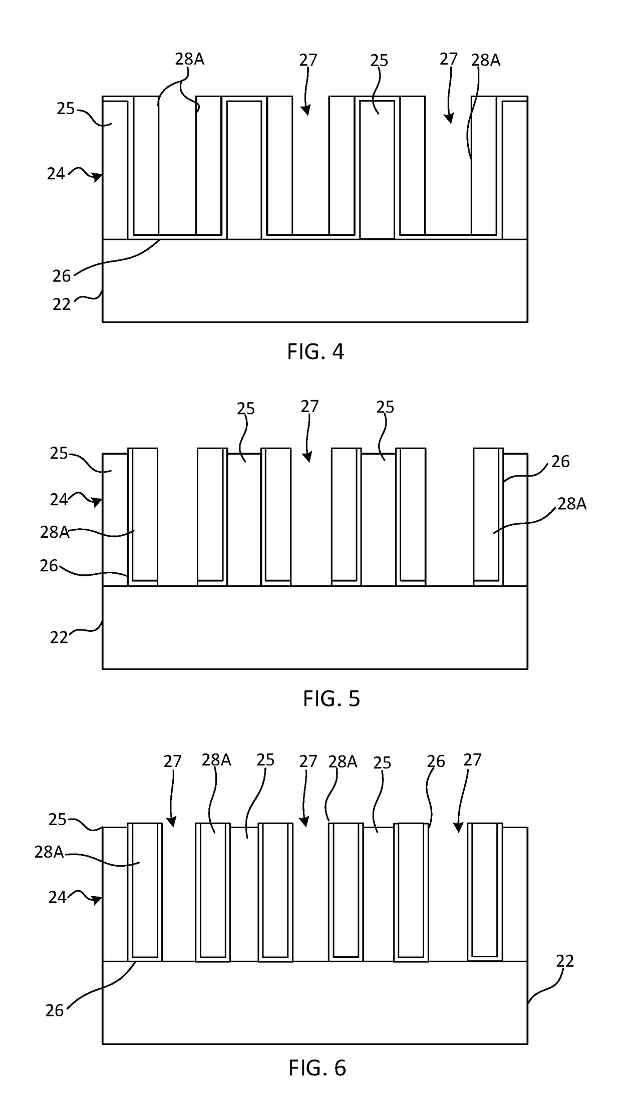
[0026]Principles of the present disclosure will be described herein in the context of illustrative embodiments. It is to be appreciated, however, that the specific embodiments and / or methods illustratively shown and described herein are to be considered exemplary as opposed to limiting. Moreover, it will become apparent to those skilled in the art given the teachings herein that numerous modifications can be made to the embodiments shown that are within the scope of the claims. That is, no limitations with respect to the embodiments shown and described herein are intended or should be inferred.

[0027]FIG. 1 schematically depicts a semiconductor structure 20 including an interconnect layer 22 and a patterned mandrel layer 24 on the interconnect layer. The interconnect layer in some embodiments is a middle-of-line (MOL) layer having contacts aligned with source / drain regions of an underlying device layer (not shown) including field-effect transistors. The patterned mandrel layer can be...


PUM

PropertyMeasurementUnit
widthaaaaaaaaaa
widthaaaaaaaaaa
thicknessaaaaaaaaaa

Abstract

A low resistance middle-of-line interconnect structure is formed without liner layers. A contact metal layer is deposited on source / drain regions of field-effect transistors and directly on the surfaces of trenches within a dielectric layer using plasma enhancement. Contact metal fill is subsequently provided by thermal chemical vapor deposition. The use of low-resistivity metal contact materials such as ruthenium is facilitated by the process. The process further facilitates the formation of metal silicide regions on the source / drain regions.

Description

BACKGROUND[0001]The present disclosure relates generally to the electrical, electronic and computer arts and, more particularly, to contact metallization processes and contact structures.[0002]With shrinking dimensions of various integrated circuit components, transistors such as FETs have experienced dramatic improvements in both performance and power consumption. These improvements may be largely attributed to the reduction in dimensions of components used therein, which in general translate into reduced capacitance, resistance, and increased through-put current from the transistors. Metal oxide semiconductor field-effect transistors (MOSFETs) are well suited for use in high-density integrated circuits. As the size of MOSFETs and other devices decreases, the dimensions of source / drain regions, channel regions, and gate electrodes of the devices, also decrease.[0003]The contribution of middle-of-line (MOL) contact resistance to the total parasitic resistance is increasing due to ag...

Claims


Application Information

Patent Timeline
Patent Type & Authority Applications(United States)
IPC IPC(8): H01L23/532H01L23/522H01L21/285H01L23/528H01L21/768H01L21/3213
CPCH01L23/53266H01L21/76877H01L21/32133H01L21/76834H01L21/7685H01L23/53252H01L21/28556H01L21/28568H01L23/528H01L23/5226H01L23/53209H01L21/76885H01L21/76852H01L23/485
Inventor ADUSUMILLI, PRANEETREZNICEK, ALEXANDERVAN DER STRATEN, OSCARYANG, CHIH-CHAO
Owner IBM CORP
Learn More