Pressure-activated electrical interconnection by micro-transfer printing

Active Publication Date: 2017-10-05
X DISPLAY CO TECH LTD
View PDF5 Cites 36 Cited by
  • Summary
  • Abstract
  • Description
  • Claims
  • Application Information

AI Technical Summary

Benefits of technology

This patent describes a method for making electrical connections between small integrated circuits and destination substrates using micro-transfer printing. The method involves heating the structure with a resin to a reflow temperature, which allows the resin to flow and wick over the substrate, components, and connection posts, creating a more intimate connection. This reduces the volume between the components and substrate, improving the electrical connection. The method is cost-effective and efficient, requiring fewer process steps than other methods. In summary, this patent provides a simple and inexpensive way to create electrical interconnections between small integrated circuits and destination substrates.

Problems solved by technology

The above techniques have some limitations.
Despite processing methods used to improve the performance of thin-film transistors, such transistors may provide performance that is lower than the performance of other integrated circuits formed in mono-crystalline semiconductor material.
Semiconductor material and active components can be provided only on portions of the substrate, leading to wasted material and processing costs.
The choice of substrate materials can also be limited by the processing steps necessary to process the semiconductor material and the photo-lithographic steps used to pattern the active components.
For example, plastic substrates have a limited chemical and heat tolerance and do not readily survive photo-lithographic processing.
Furthermore, the manufacturing equipment used to process large substrates with thin-film circuitry is relatively expensive.
However, such substrate materials can be more expensive or difficult to process.
However, these techniques may be limited in the size of the integrated circuits that can be placed.
While this approach can provide substrates with the same performance as integrated circuits, the size of such substrates may be limited, for example, to a 12-inch diameter circle, and the wafers are relatively expensive compared to other substrate materials such as glass, polymer, or quartz.
However, the bonding technique and the processing equipment for the substrates to form the thin-film active components on large substrates can be relatively expensive.
This method may require etching a significant quantity of material, and may risk damaging the exposed TFT array.
These methods, however, may require the patterned deposition of adhesive on the object(s) or on the second substrate.
Moreover, the laser beam that irradiates the object may need to be shaped to match the shape of the object, and the laser abrasion can damage the object to be transferred.
Furthermore, the adhesive cure takes time, which may reduce the throughput of the manufacturing system.
This process is expensive and requires a number of manufacturing steps.
Moreover, the topographical structure of the small integrated circuits over the destination substrate renders the electrical connections problematic.
For example, it can be difficult to form a continuous conductor from the destination substrate to the small integrated circuit because of the differences in height over the surface between the small integrated circuits and the destination substrate.

Method used


Image

  • Pressure-activated electrical interconnection by micro-transfer printing
  • Pressure-activated electrical interconnection by micro-transfer printing
  • Pressure-activated electrical interconnection by micro-transfer printing

Examples


Embodiment Construction

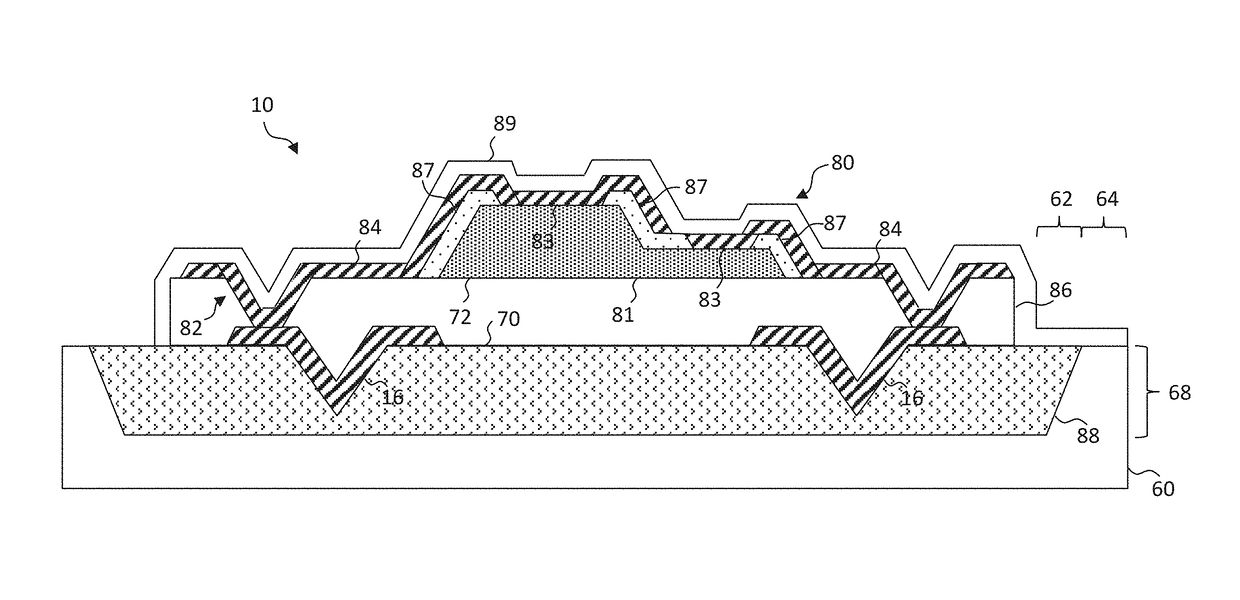
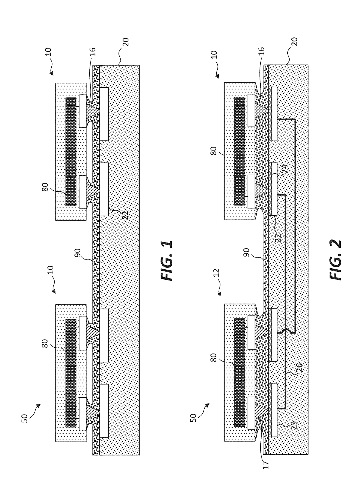
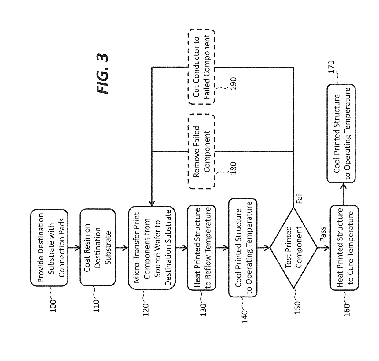
[0113]The present invention provides a structure and method for electrically connecting relatively small electrical components such as integrated circuit chiplets, LEDS, or electrical jumpers to a relatively large destination substrate in an efficient and cost-effective way. Referring to FIGS. 1 and 2 in an embodiment of the present invention, a printed electrical connection structure 50 includes a substrate 20 having one or more electrical connection pads 22 formed on or in the substrate 20. The connection pads 22 can be, for example metal backplane contact pads made using photolithographic methods, tools, and materials. The substrate 20 can be, for example, a printed circuit board or display substrate and can include glass, polymer, plastic, resin, or fiber glass.

[0114]A printed component 10 has a circuit 80 and one or more connection posts 16. The circuit 80 can be any structure responsive to, controlling, or conducting electrical energy supplied through the connection posts 16, ...


PUM


Abstract

A printed electrical connection structure includes a substrate having one or more electrical connection pads and a micro-transfer printed component having one or more connection posts. Each connection post is in electrical contact with a connection pad. A resin is disposed between and in contact with the substrate and the component. The resin has a reflow temperature less than a cure temperature. The resin repeatedly flows at the reflow temperature when temperature-cycled between an operating temperature and the reflow temperature but does not flow after the resin is exposed to a cure temperature. A solder can be disposed on the connection post or the connection pad. After printing and reflow, the component can be tested and, if the component fails, another component is micro-transfer printed to the substrate, the resin is reflowed again, the other component is tested and, if it passes the test, the resin is finally cured.

Description

PRIORITY APPLICATION[0001]This application claims priority to and benefit of U.S. Patent Application No. 62 / 317,107, filed Apr. 1, 2016, entitled Pressure-Activated Electrical Interconnection by Micro-Transfer Printing, the content of which is hereby incorporated by reference in its entirety.CROSS REFERENCE TO RELATED APPLICATION[0002]Reference is made to U.S. Pat. No. 8,889,485, entitled Methods for Surface Attachment of Flipped Active Components by Christopher Bower, to U.S. patent application Ser. No. 14 / 822,864, entitled Chiplets with Connection Posts by Prevatte et al, to U.S. patent application Ser. No. 14 / 743,788, entitled Micro Assembled LED Displays and Lighting Elements by Bower et al., and to U.S. patent application Ser. No. 15 / 373,865, entitled Micro-Transfer Printable Electronic Component by Cok et al., the disclosures of which are incorporated herein by reference in their entirety.FIELD OF THE INVENTION[0003]The present invention relates to structures and methods for e...

Claims


Application Information

Patent Timeline
IPC IPC(8): H01L21/66H01L33/62H01L33/56
CPCH01L22/12H01L27/3255H01L33/62H01L33/56H01L2224/75305H01L2224/13008H01L22/22H01L24/11H01L24/13H01L24/81H01L24/83H01L24/92H01L24/97H01L25/50H01L27/1266H01L2224/13013H01L2224/13016H01L2224/16237H01L2224/75315H01L2224/81191H01L2224/814H01L2224/81815H01L2224/8182H01L2224/81986H01L2224/83192H01L2224/83862H01L2224/83986H01L2224/9211H01L2224/95136H01L2224/7598H01L2224/1411H01L2224/81903H01L2224/02123H01L2224/951H01L22/14H01L22/20H01L25/167H01L27/156H01L33/38H01L2224/95001H01L2224/97H01L27/124H01L24/98H10K71/611H10K10/82H10K50/805H10K59/1201H01L2224/81H01L2224/83H01L2924/014H10K59/129
Inventor BOWER, CHRISTOPHER ANDREWCOK, RONALD S.MEITL, MATTHEWPREVATTE, JR., CARL RAY
Owner X DISPLAY CO TECH LTD
Why Eureka
Try Eureka