Composite solder transfer moldplate structure and method of making same

a technology of composite solder transfer and moldplate, which is applied in the direction of soldering equipment, manufacturing tools,auxillary welding devices, etc., can solve the problems of reworking or discarded parts, significant challenges in the production of borosilicate glass solder transfer moldplates, and defect-prone key processing steps. achieve the effect of simple and inexpensive process and easy production

Inactive Publication Date: 2006-12-28
BUCHWALTER STEPHEN L +5
View PDF14 Cites 18 Cited by
  • Summary
  • Abstract
  • Description
  • Claims
  • Application Information

AI Technical Summary

Benefits of technology

[0013] It is therefore an aspect of the present invention to provide a moldplate that is made by a simple and inexpensive process, is robust and is easily produced.

Problems solved by technology

However, there are also significant challenges to producing borosilicate glass solder transfer moldplates.
Especially as the number of cavities increase and the cavity dimensions decrease, several of the key processing steps are prone to defects that affect the completed moldplate quality.
Photolithographic tooling is required for typically fine cavity dimensions involving costly masks to define the initial locations of cavities that will be chemically etched.
Thus, if there is a defect with any of the processing steps, the part must be either reworked or discarded.
More processing steps increase the risk of such defects and affect the overall yield of the process.
All these requirements increase the challenge of making defect free moldplates with the conventional process.

Method used


Image

  • Composite solder transfer moldplate structure and method of making same
  • Composite solder transfer moldplate structure and method of making same
  • Composite solder transfer moldplate structure and method of making same

Examples


example

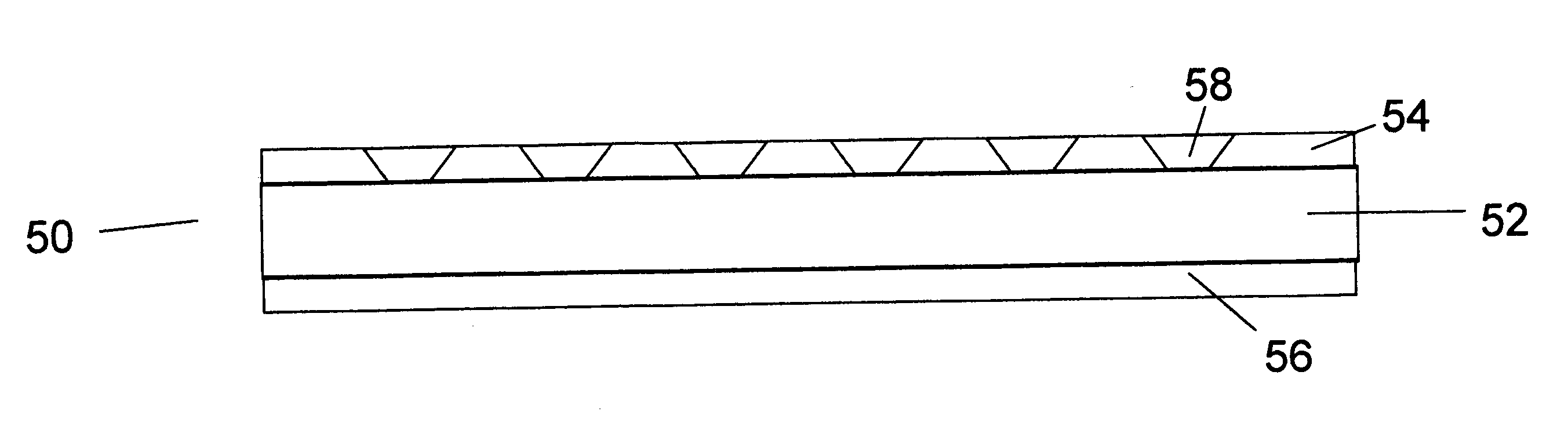
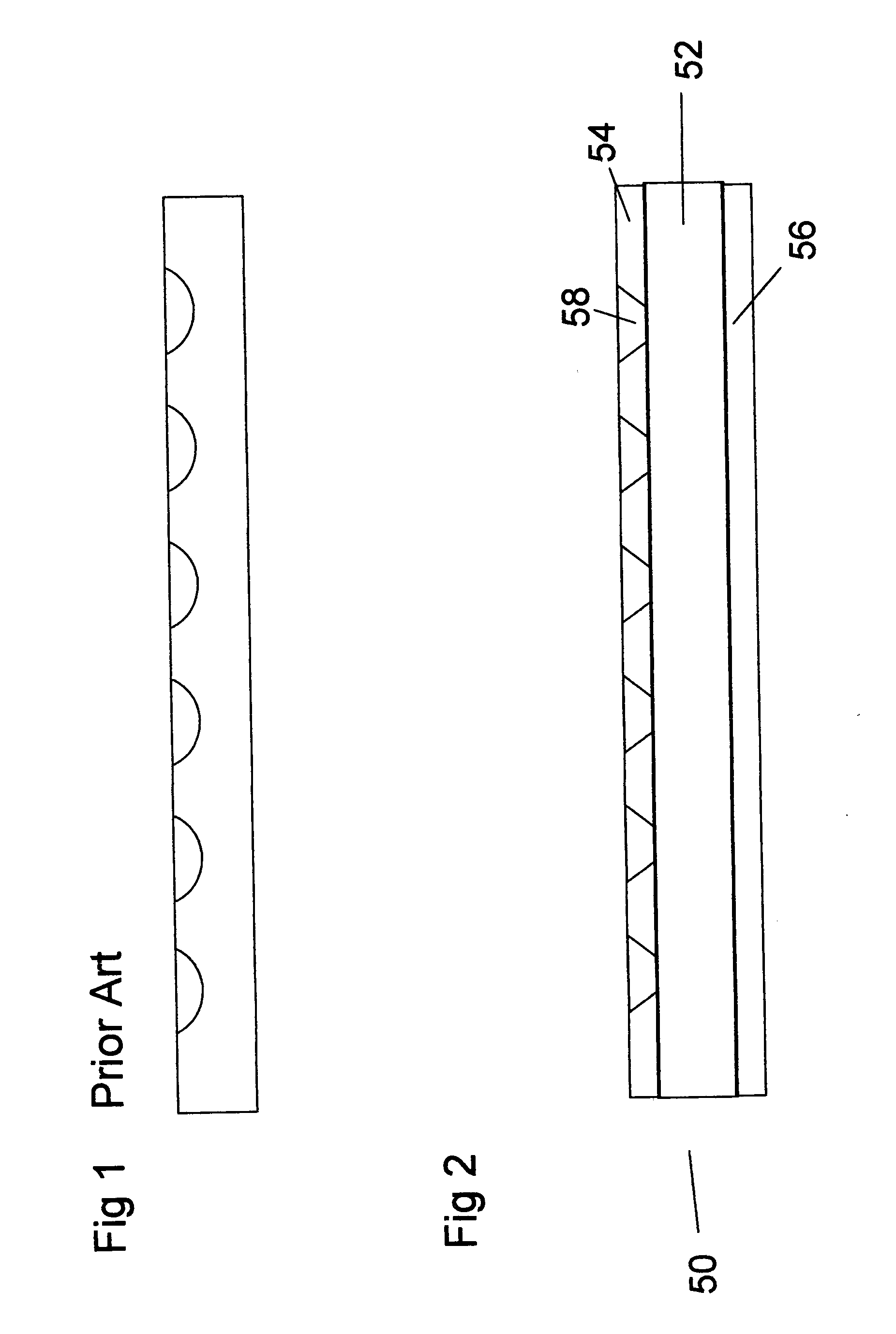
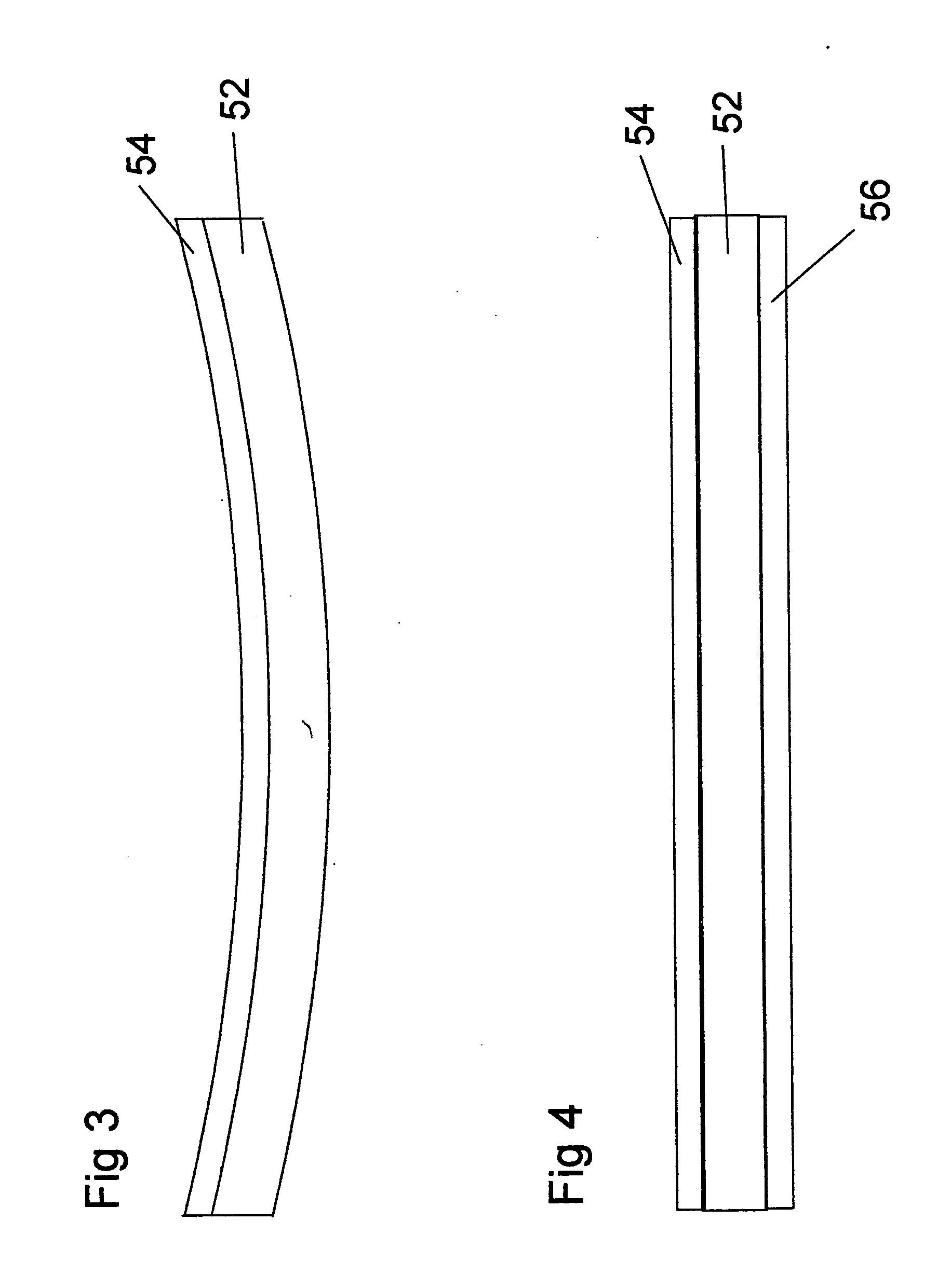
[0063] It has been found that whereas conventional glass solder transfer moldplates require substantial effort to achieve defect-free cavity densities of 0.004 inch (0.1 mm) diameter cavities on 0.008 inch (0.2 mm) centers, laser-drilled composite solder transfer moldplates have readily achieved finer 0.003 inch (0.08 mm) diameter cavities on 0.006 inch (0.15 mm) centers without defects. Thus, the extendibility of this simplified composite structure is demonstrated.

[0064] Since an important aspect of this invention deals with the cavities in the composite solder transfer moldplate structure, details of the laser machining process used to produce the cavities are provided below.

[0065] Laser drilling is performed on a ESI 5210 Laser Microvia System provided by Electo Scientific Industries, Inc. of Portland, Oreg. A frequency-tripled Nd:YAG laser operating at a wavelength of 355 nanometers is used. The pulse width of the laser is on the order of 50 nanoseconds. The output of the lase...


PUM

PropertyMeasurementUnit
wavelengthaaaaaaaaaa
poweraaaaaaaaaa
thicknessaaaaaaaaaa

Abstract

A method for constructing a composite solder transfer moldplate for flip chip wafer bumping of a substrate, comprising the steps of coating at least one polymer layer onto a first side of a transparent plate, the plate having a thermal expansion coefficient similar to that of the substrate; and forming a multiplicity of cavities in a polymer layer on one side of the plate, each cavity being for receiving solder. A moldplate made by the method. The structure has required behavior through temperature excursions between room temperature and various solder molten temperatures.

Description

FIELD OF THE INVENTION [0001] The present invention relates to a method for providing moldplates used in flip chip wafer bumping, and to moldplates produced by the method. More particularly, it relates to a method for building composite moldplates by coating substrate plates, and machining these coated layers, and to the moldplates produced. BACKGROUND OF THE INVENTION [0002] As seen in FIG. 1, previously solder transfer moldplates had blind holes or cavities placed directly within the glass that typically comprised such structures. Since electronic wafers are usually made of silicon, the glass used to transfer the solder deposited by injection molded solder (IMS) is carefully chosen to closely match the coefficient of thermal expansion (CTE) of silicon (2.3 10−6 / degree C.). Borosilicate glass provides such a CTE match and has several additional desirable attributes. Included in these is the ability to chemically etch cavities in the glass and transparency for optical alignment betw...

Claims


Application Information

Patent Timeline
Patent Type & Authority Applications(United States)
IPC IPC(8): B23K35/12
CPCB23K35/3613
Inventor BUCHWALTER, STEPHEN L.DANOVITCH, DAVIDEGITTO, FRANK D.GRUBER, PETER A.PERFECTO, ERIC D.SHIH, DA-YUAN
Owner BUCHWALTER STEPHEN L
Why Eureka
Try Eureka