Unlock instant, AI-driven research and patent intelligence for your innovation.

Method of manufacturing light scattering layer and organic light-emitting diode

Active Publication Date: 2017-10-12
WUHAN CHINA STAR OPTOELECTRONICS TECH CO LTD
View PDF0 Cites 1 Cited by
  • Summary
  • Abstract
  • Description
  • Claims
  • Application Information

AI Technical Summary

Benefits of technology

The present invention provides a method for manufacturing a light scattering layer for an organic light-emitting diode (OLED) that overcomes the technical problem of complicated manufacturing processes, uncontrollable scattering effect, and high manufacturing cost caused by avoiding the presence of a wave guide mode. The manufacturing process involves using a mask with plurality of hole structures to create raised structures on a base, which are then planarized to form a light scattering layer. The resulting light scattering layer has controlled scattering effect and enhanced light extraction efficiency of the OLED. The OLED with the light scattering layer has substantially reduced presence of the wave guide mode and enhanced light extraction efficiency. This method is simple and cost-effective, and allows for mass production of scattering layers with different scattering effects. Additionally, the OLED with the light scattering layer has improved light extraction efficiency.

Problems solved by technology

However, when the light propagates through the OLED device, a plurality of modes, such as plasma mode, wave guide mode, and substrate mode, are presented, and cannot be avoided.
These modes result in that the light from the OLED device cannot be highly efficiently coupled into air, thereby restricting the efficiency of the light emission of the OLED.
In these modes mentioned above, the main factor restricting the efficiency of the light emission of the OLED is the wave guide mode.
However, the manufacturing process is complicated and expensive.
Due to the photonic crystals with different periods need to be manufactured by different stamping moldings, the manufacturing cost will be increased.
The light scattering layer is a SiO2 layer with low refractive index and a grid structure, and is manufactured by a photolithography process; notwithstanding the light scattering layer can achieve reducing the wave guide mode, the manufacturing process is complicated and it is difficult to control parameters caused from the organic layers being stacked with a waved configuration.
Moreover, the light scattering layer located between the ITO and the glass base is doped with low refractive index particles and bubbles which have different masses and sizes; there are great differences between these particles, so it is difficult to control the light scattering effect.

Method used


Image

  • Method of manufacturing light scattering layer and organic light-emitting diode
  • Method of manufacturing light scattering layer and organic light-emitting diode
  • Method of manufacturing light scattering layer and organic light-emitting diode

Examples


Embodiment Construction

[0057]Referring to the drawings, a same component symbol represents a same component. The following descriptions are based on illustrated specific embodiments of the present invention, and should not be regarded as limitations on other specific embodiments of the present invention that are not described in detail herein.

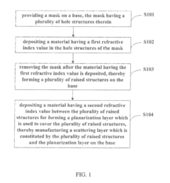
[0058]Please refer to FIG. 1, which is a flow chart of a method of manufacturing a light scattering layer in accordance with a first preferred embodiment of the present invention. The manufacturing method comprises:

[0059]Step S101, providing a mask on a base, the mask having a plurality of hole structures therein;

[0060]Step S102, depositing a material having a first refractive index value in the hole structures of the mask;

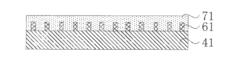
[0061]Step S103, removing the mask after the material having the first refractive index value is deposited, thereby forming a plurality of raised structures on the base;

[0062]Step S104, depositing a material having a second refractive index value b...


PUM


Abstract

A method of manufacturing a light scattering layer and an organic light-emitting diode are provided. The manufacturing method includes: depositing a material having a low refractive index value in hole structures of a mask on a base; removing the mask, and forming a plurality of raised structures on the base; depositing a material having a high refractive index value between the raised structures to form a planarization layer, thereby manufacturing a light scattering layer constituted by the raised structures and the planarization layer on the base. The manufacturing method has the advantages of being simple to prepare, low-cost, etc.

Description

FIELD OF THE INVENTION[0001]The present invention relates to the field of display technology, and more particularly to a method of manufacturing a light scattering layer and an organic light-emitting diode having the light scattering layer manufactured by the method.BACKGROUND OF THE INVENTION[0002]Organic Light-Emitting Diode (OLED) is a display technology with self-light emitting characteristics, and it uses extremely thin organic material coating and glass substrate. When current passes therethrough, the organic material will emit light. Since the OLED has several advantages, such as high contrast degree, wide viewing angle, low power consumption, simple structure, lightweight, and flexible, it is gradually replacing thin-film-transistor liquid crystal displays (TFT-LCD) and has received the most attention recently.[0003]However, when the light propagates through the OLED device, a plurality of modes, such as plasma mode, wave guide mode, and substrate mode, are presented, and ca...

Claims


Application Information

Patent Timeline
IPC IPC(8): H01L51/52H01L51/56
CPCH01L51/5268H01L2251/301H01L51/56H10K71/166H10K50/854H10K2102/103H10K71/00H10K2102/00
Inventor WU, ZHIYONGXU, LIANG
Owner WUHAN CHINA STAR OPTOELECTRONICS TECH CO LTD