Method of manufacturing semiconductor device

a manufacturing method and semiconductor technology, applied in semiconductor devices, chemical vapor deposition coatings, coatings, etc., can solve the problems of high resistivity of an obtained metal film and low resistivity of a metal film, and achieve the effect of reducing roughness and low resistivity

Pending Publication Date: 2017-10-26
KOKUSA ELECTRIC CO LTD
View PDF119 Cites 165 Cited by
  • Summary
  • Abstract
  • Description
  • Claims
  • Application Information

AI Technical Summary

Benefits of technology

[0006]The present invention provides a technique that enables formatio

Problems solved by technology

In addition, a low resistivity is demanded of a metal film.
However, when using a non-crystalline (amorphous) film in order to reduce surfa

Method used


Image

  • Method of manufacturing semiconductor device
  • Method of manufacturing semiconductor device
  • Method of manufacturing semiconductor device

Examples


first embodiment

of the Present Invention

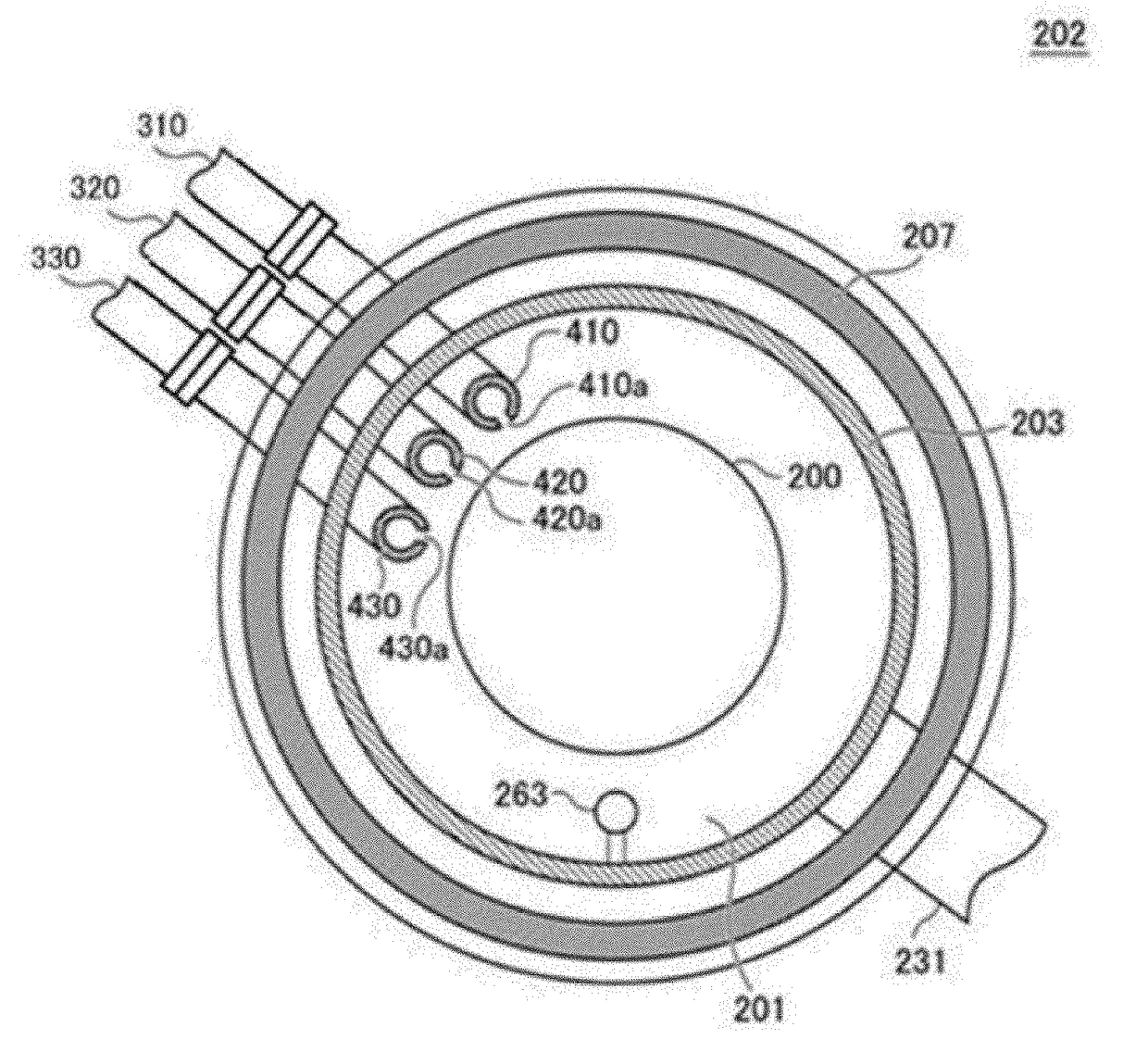
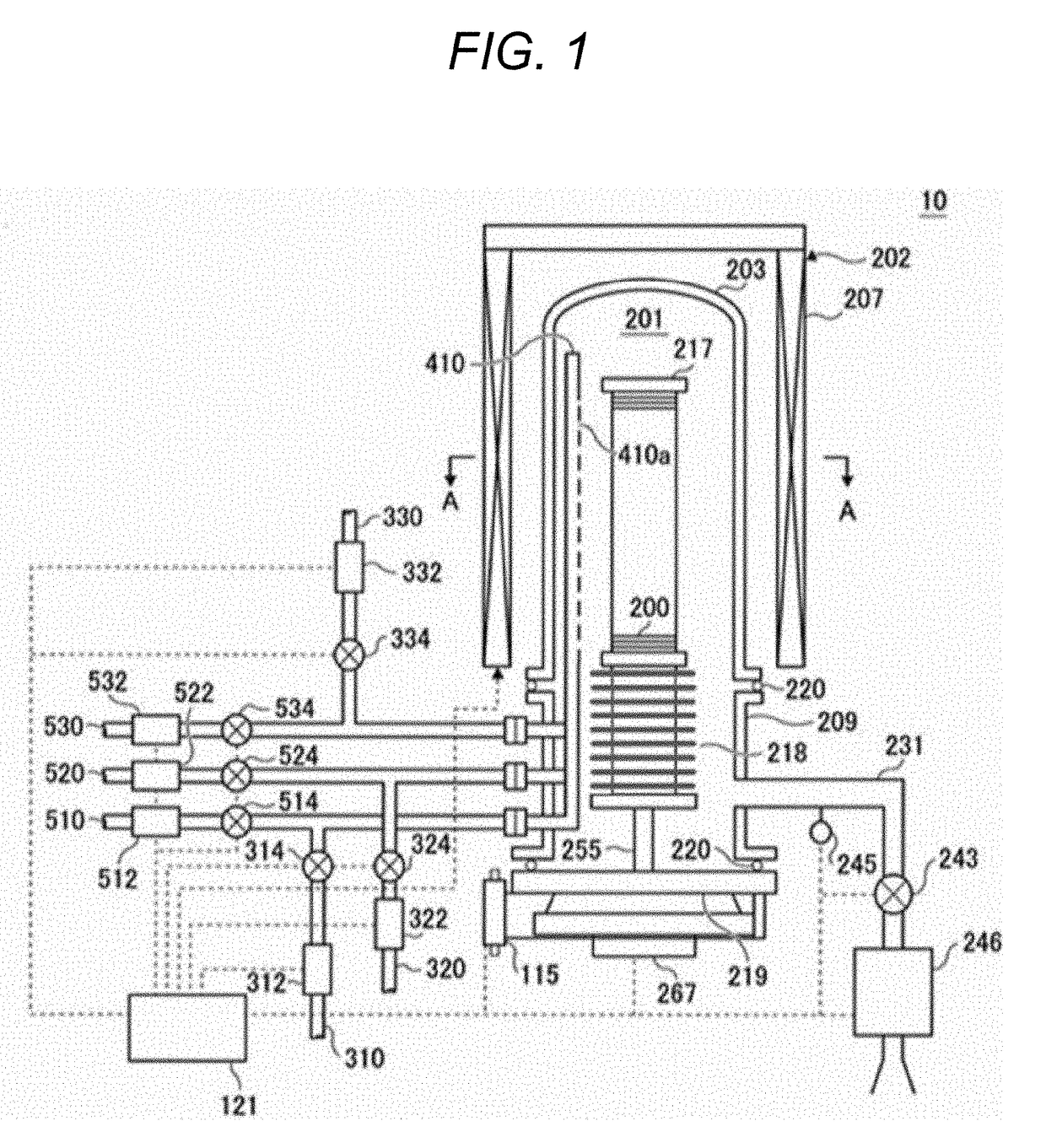
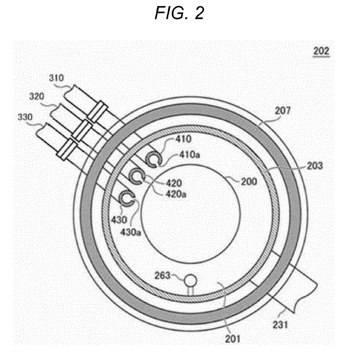
[0017]In the following, a first embodiment of the present invention will be described with reference to FIG. 1 and FIG. 2. A substrate processing apparatus 10 is configured as one example of an apparatus for use in a substrate processing step which is one step of semiconductor device manufacturing steps.

[0018](1) Configuration of Processing Furnace

[0019]A processing furnace 202 is provided with a heater 207 as heating means (a heating mechanism, a heating system). The heater 207 is formed to have a cylindrical shape with an upper portion opened.

[0020]On an inner side of the heater 207, a reaction tube 203 is disposed which configures a reaction container (processing container) so as to be concentrical with the heater 207. The reaction tube 203 is made of a heat-resistant material or the like (e.g. quartz (SiO2) or silicon carbide (SiC)) and is formed to be cylindrical with an upper end thereof blocked and a lower end thereof opened.

[0021]To a lower end of the...

second embodiment

of the Present Invention

[0115]In the first embodiment, the description has been made of an example in which as a bulk layer, an α-W film is formed by combining a first α-W layer and a second α-W layer, on which film, a crystallized W layer is formed, thereby forming a crystallized W film with a desired film thickness by low temperature processing at 250° C. or less and preferably 200° C. or less. In the present embodiment, description will be made, with reference to FIG. 6, of an example where as a base of the above-described bulk layer, the tungsten film (W film) 503 is formed as a seed layer formed on the TiN film 502 formed as a barrier metal film. No detailed description will be made of the same part as the first embodiment, and a part different from the first embodiment will be described in the following.

[0116](Seed W Film Forming Step)

[0117]A W film as a seed layer (a seed W film) is formed by executing a seed W film forming step including a WF6 gas supply step, a residual gas...


PUM

PropertyMeasurementUnit
Temperatureaaaaaaaaaa

Abstract

A method of manufacturing a semiconductor device includes: forming an amorphous metal film on a substrate by time-divisionally conducting a cycle a predetermined number of times, the cycle including: (a) simultaneously supplying a metal-containing gas and a first reducing gas to the substrate to form a first amorphous metal layer on the substrate, and (b) forming a second amorphous metal layer on the first amorphous metal layer by time-divisionally supplying, a predetermined number of times, the metal-containing gas and a second reducing gas to the substrate on which the first amorphous metal layer is formed; and forming a crystallized metal layer on the substrate by simultaneously supplying the metal-containing gas and the first reducing gas to the substrate on which the amorphous metal film is formed.

Description

TECHNICAL FIELD[0001]The present invention relates to a method of manufacturing a semiconductor device in which a thin film is formed on a substrate.BACKGROUND ART[0002]In recent years, with an increase in circuit integration and improvement in performance, it is demanded to form a metal film in an extra fine groove having a narrower than conventional opening portion. In addition, a low resistivity is demanded of a metal film. Applications of such a metal film include, for example, applications to control gate of a flash memory, to a gate electrode of a DRAM (Dynamic Random Access Memory), to wiring between electrodes, and the like.SUMMARY[0003]When embedding a metal film in an opening portion, use of a crystallized film increases surface roughness (also referred to simply as roughness) to generate a void in some cases. However, when using a non-crystalline (amorphous) film in order to reduce surface roughness, a temperature at the time of film formation should be low, resulting in ...

Claims


Application Information

Patent Timeline
IPC IPC(8): H01L21/285C23C16/455C23C16/06C23C16/34
CPCH01L21/28556C23C16/45525H01L21/28568C23C16/45527C23C16/34C23C16/06C23C16/14C23C16/45529H01L21/28562H01L21/76876H01L21/76877H01L29/401H01L21/76843H01L29/4966C23C16/0281H01L29/435H01L29/42372
Inventor OGAWA, ARITO
Owner KOKUSA ELECTRIC CO LTD
Why Eureka
Try Eureka