


Quick Research
Generate reliable direction feasibility study reports for your R&D in just a few steps.

Technical Q&A
Discover and master advanced knowledge NOW. Basics, ideas, possibilities, all at once.

Find Solutions
As an expert in R&D theories, this can generate solutions to your technical problems instantly.

Evaluate Feasibility
Analyze your overall solution with one click, know your potential R&D risks in advance.

Monitor Landscape
Get weekly tech updates, stay abreast of the latest tech innovations and key insights.
Method of manufacturing electroformed components
a manufacturing method and technology of electroformed components, applied in the field of electroformed component manufacturing, can solve the problems of poor manufacturing efficiency, difficult to ensure the manufacturing accuracy of the portions, and poor manufacturing efficiency of the above-mentioned manufacturing methods
- Summary
- Abstract
- Description
- Claims
- Application Information
AI Technical Summary
Benefits of technology
Problems solved by technology
Method used
Image


Examples
first embodiment
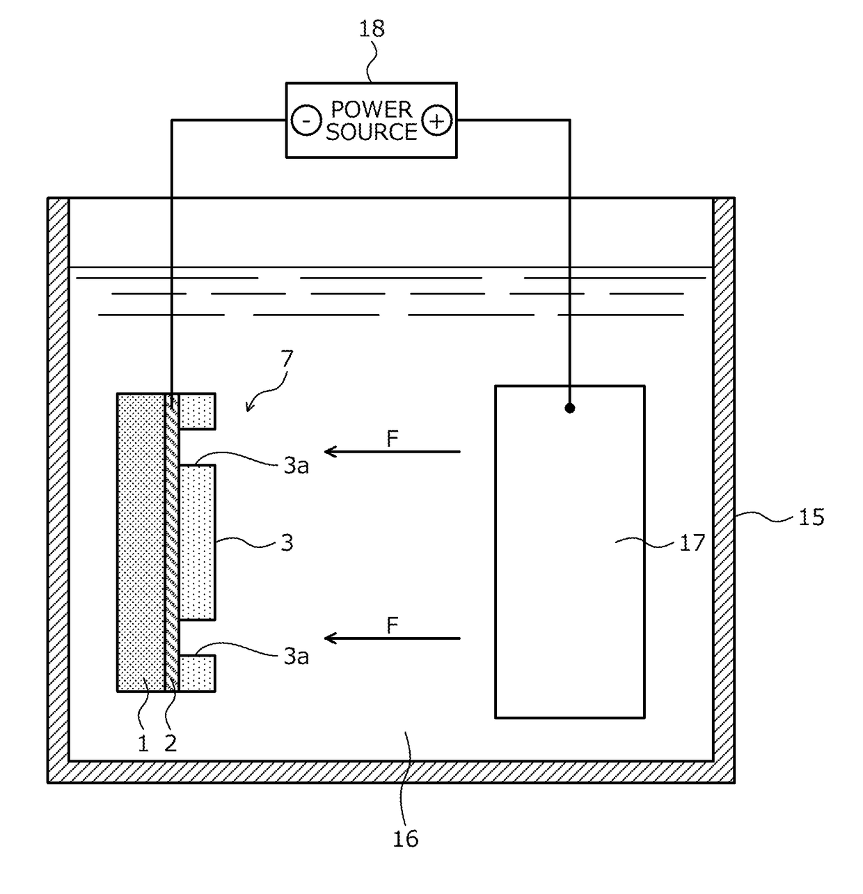
[0080]In a first embodiment, a method of manufacturing electroformed components achieved by application of a lithographie, galvanoformung, abformung (LIGA) method will be described as a method of manufacturing electroformed components of a first embodiment according to the present invention. The LIGA method is a method of manufacturing a target part (structure) by combining X-ray lithography, electroforming, and molding, and is capable of manufacturing a component having a large aspect ratio (ratio of depth (height) to processing width).
[0081]When an electroformed component is manufactured using the LIGA method, a resist (photosensitive organic material) having a thickness of 100 μm or more is exposed to X-rays through a mask (X-ray mask) to transfer a pattern of the mask to the resist. This enables manufacturing of a component having a depth (height) of 100 μm or more and an arbitrary shape in a lateral direction (direction along a surface of a substrate). Preferably, the X-rays to...
second embodiment
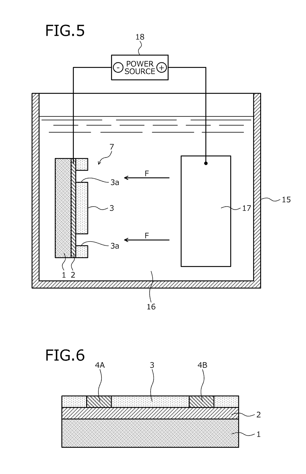
[0130]A method of manufacturing electroformed components of a second embodiment according to the present invention will be described. In the second embodiment, portions identical to those in the first embodiment described above are denoted by the same reference characters used in the first embodiment and will not be described. FIGS. 16, 17, 18, 19, 20, 21, and 22 are explanatory views of a portion of a procedure of manufacturing electroformed components according to the method of manufacturing electroformed components of the second embodiment according to the present invention. In the procedure of manufacturing electroformed components according to the method of manufacturing electroformed components of the second embodiment, steps identical to the steps depicted in FIGS. 1 to 4 and 6 described above are executed, and steps depicted in FIGS. 16 to 22 are subsequently executed.
(Procedure of Manufacturing Electroformed Components)
[0131]In manufacturing of electroformed components acco...
third embodiment
[0151]A method of manufacturing electroformed components of a third embodiment according to the present invention will be described. In the third embodiment, portions identical to those in the first and second embodiments described above are denoted by the same reference characters used in the first and second embodiments and will not be described. FIGS. 23, 24, 25, 26, 27, 28, 29, 30, 31, 32, and 33 are explanatory views of a procedure of manufacturing electroformed components according to the method of manufacturing electroformed components of the third embodiment according to the present invention.
(Procedure of Manufacturing Electroformed Components)
[0152]In the manufacturing of electroformed components according to the method of manufacturing electroformed components of the third embodiment, first, as depicted in FIG. 23, a substrate 10 is prepared. The substrate 10 may be formed using a conductive material having favorable conductivity, for example. For example, the substrate 1...
PUM
| Property | Measurement | Unit |
|---|---|---|
| thickness | aaaaa | aaaaa |
| height | aaaaa | aaaaa |
| thickness | aaaaa | aaaaa |
Abstract
Description
Claims
Application Information
 - R&D Engineer
- R&D Manager
- IP Professional
- Industry Leading Data Capabilities
- Powerful AI technology
- Patent DNA Extraction
Browse by: Latest US Patents, China's latest patents, Technical Efficacy Thesaurus, Application Domain, Technology Topic, Popular Technical Reports.
© 2024 PatSnap. All rights reserved.Legal|Privacy policy|Modern Slavery Act Transparency Statement|Sitemap|About US| Contact US: help@patsnap.com